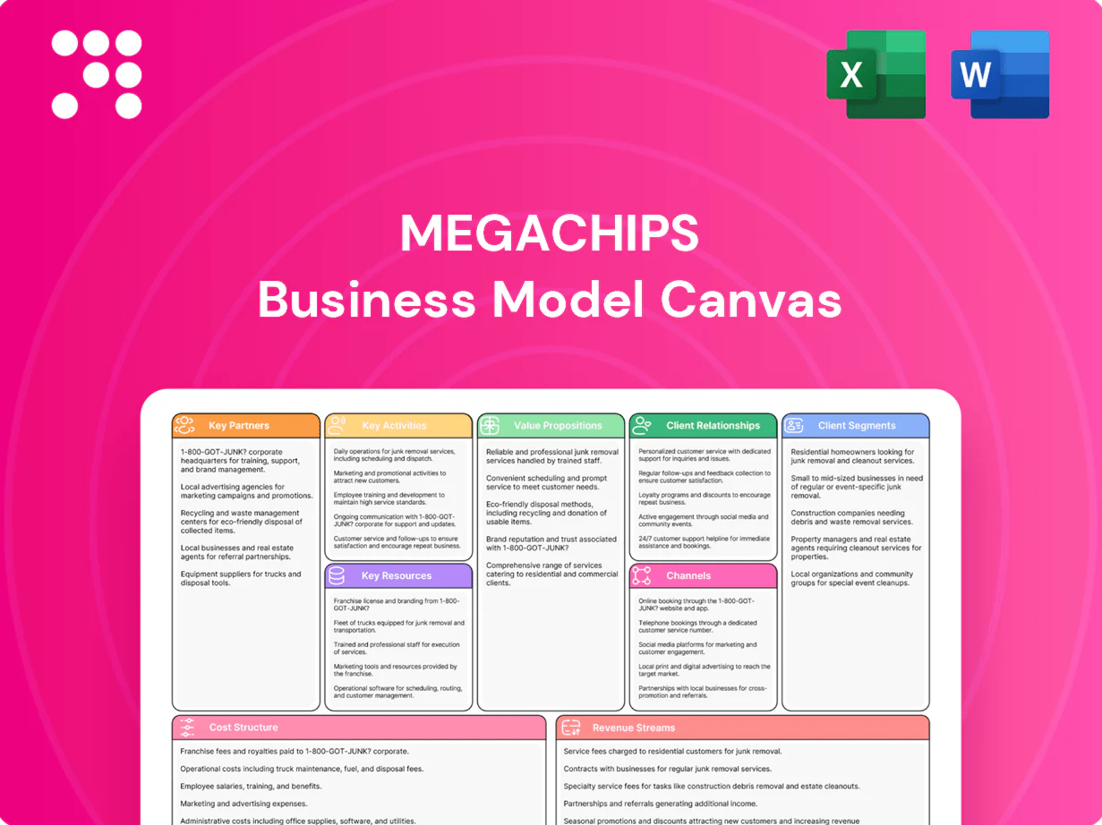
MegaChips Business Model Canvas

Business Model Canvas: Strategic Blueprint for Semiconductor Growth and Revenue Capture
Unlock the full strategic blueprint behind MegaChips with our in-depth Business Model Canvas — three to five concise sections reveal how the company creates value, scales operations, and captures revenue in a competitive semiconductor ecosystem. Perfect for investors, consultants, and founders, the downloadable Word and Excel files give a ready-to-use template for benchmarking and planning. Purchase the full Canvas to dissect every building block and turn insight into action.
Partnerships

Foundry and OSAT alliances
As a fabless supplier, MegaChips depends on foundry and OSAT alliances for wafer fab and back-end test/packaging; securing multi-node capacity and advanced packaging (heterogeneous integration) is critical for cost and performance. With TSMC holding >50% foundry share in 2024 and the global OSAT market exceeding US$40B in 2024, long-term agreements reduce supply risk and joint DFM/DFT collaboration shortens time-to-yield and improves unit economics.
EDA and IP ecosystem partners
Access to best-in-class EDA tools and licensed IP shortens RTL-to-GDS timelines and lowers integration risk; the global EDA market exceeded $12 billion in 2024, underscoring tool importance. CPU cores, interface PHYs and connectivity stacks cut development time and reuse effort, while co-optimization with EDA vendors sharpens PPA and verification coverage. Preferred-pricing and roadmap visibility from partners improve MegaChips competitiveness.

OEM/ODM co-development partners
Close collaboration with OEM/ODM co-development partners anchors design wins and volume commitments, while joint requirements capture steers custom SoC and ASIC features to OEM specs. Early access to device roadmaps lets MegaChips align silicon schedules with product launches. Co-validation with partners shortens integration cycles and speeds time-to-market.

Standards bodies and module vendors
Standards bodies and module vendors ensure MegaChips devices comply with imaging, audio and connectivity protocols; participation with bodies such as the Wi‑Fi Alliance and Bluetooth SIG in 2024 keeps designs aligned with current specs and reduces redesign risk. Early access to evolving specs lowers integration costs and module partners accelerate adoption in end systems, while certification partners streamline entry to global markets.
- Standards alignment: JEITA, Wi‑Fi Alliance, Bluetooth SIG (2024)
- Redesign risk: reduced via early spec access
- Faster adoption: module partners speed integration
- Market access: certification partners ease global rollout
Supply chain and logistics providers
MegaChips leverages global distribution across 45 countries and 12 regional inventory hubs; collaborative forecasting lifted on-time deliveries by 18% in 2024 while risk-managed buffers (≈20% surge capacity) support aggressive ramp profiles. Quality and traceability systems aligned to ISO and industry traceability standards ensure compliance; cost-optimized freight saved about $14M in 2024, protecting margins.
- Global reach: 45 countries
- Hubs: 12 regions
- Forecast lift: +18% OTIF (2024)
- Buffer: ~20% surge capacity
- Freight savings: $14M (2024)
Foundry & OSAT ties, EDA/IP and 45-country distro lift OTIF +18%
MegaChips relies on foundry/OSAT alliances (TSMC >50% foundry share; OSAT market >$40B in 2024) for capacity and advanced packaging, long-term agreements cut supply risk. EDA/IP partners (EDA market ~$12B in 2024) accelerate RTL-to-GDS and improve PPA. OEM/ODM, standards and distro (45 countries, 12 hubs) secure design wins, lift OTIF +18% and saved $14M freight in 2024.
| Partner Type | Key Metric | 2024 |
|---|---|---|
| Foundry/OSAT | Market/Share | OSAT>$40B; TSMC>50% |
| EDA/IP | Market | $12B |
| Distribution | Reach/OTIF/Savings | 45 countries; 12 hubs; OTIF+18%; $14M |
What is included in the product
 Detailed Word Document
A concise, pre-written Business Model Canvas tailored to MegaChips’ strategy, covering customer segments, channels, value propositions, key activities, partners, resources, revenue streams and cost structure across 9 BMC blocks. Ideal for presentations and investor discussions, it links competitive advantages and SWOT insights to real-world operations for informed decision-making.

 Customizable Excel Spreadsheet
High-level, editable Business Model Canvas for MegaChips that condenses complex semiconductor strategy into a one-page, shareable snapshot—ideal for teams to quickly relieve strategic alignment and communication pain points.
Activities

Custom SoC/ASIC design
Custom SoC/ASIC design delivers end-to-end architecture, RTL-to-GDSII physical implementation tailored to target use-cases, integrating imaging, audio and connectivity IP blocks with DFT insertion and signoff achieving >95% test coverage; iterative PPA optimization targets customer KPIs, typically delivering up to 20% combined power/performance/area gains while meeting manufacturability and time-to-market constraints.
Verification and validation
Verification and validation use constrained-random, formal methods, and emulation to secure functional correctness across designs, targeting >95% functional coverage; emulation accelerates bug discovery pre-silicon. Hardware bring-up occurs on evaluation boards and reference platforms to shorten first-silicon debug cycles by ~30%. Compliance and interoperability testing covers industry standards such as PCIe, USB, and MIPI. Regression automation runs nightly suites (~10,000 tests) to maintain quality.

Firmware and software enablement
Device drivers, SDKs and reference stacks enable rapid design-in for MegaChips, shortening integration cycles and enabling quicker time-to-market.
Imaging pipelines, audio processing blocks and connectivity middleware (Wi‑Fi/BLE/BT) are provided as production-ready modules to accelerate product development.
BSPs cover major OS/RTOS as of 2024 — Linux, Android, FreeRTOS and ThreadX — with continuous updates and long-term maintenance to support customer products.

Productization and quality
MegaChips ensures industrial and communication-grade qualification using AEC-Q100, ISO 26262 and JEDEC JESD47 standards as of 2024; reliability testing employs HALT/HASS, accelerated stress and root-cause failure analysis driving corrective actions. Yield improvement focuses on test-program optimization and SPC to lower escapes; lifecycle management and PCN control follow JEDEC/IEC industry practices.
- Standards: AEC-Q100, ISO 26262, JEDEC JESD47
- Reliability: HALT/HASS, FA-driven CA
- Yield: test optimization, SPC
- Lifecycle: PCN per JEDEC/IEC
Customer support and field enablement
MegaChips in 2024 deploys FAEs from concept to production, running formal design reviews, SI/PI guidance, and shipping reference designs to accelerate time‑to‑market and improve first‑pass success rates.
Comprehensive training, documentation, and application notes are issued alongside sustaining engineering for multi‑year programs to ensure product longevity and compliance with customer lifecycle requirements.
RTL-to-GDSII SoC: >95% coverage, 20% PPA gains
Custom SoC/ASIC design delivers end-to-end RTL‑to‑GDSII with >95% test coverage and up to 20% combined PPA gains, meeting manufacturability and TTM targets.
Verification/emulation and nightly ~10,000-test regressions shorten first‑silicon debug ~30%; BSPs cover Linux, Android, FreeRTOS, ThreadX (2024).
FAEs support concept→production; reliability per AEC‑Q100, ISO 26262, JEDEC JESD47 with HALT/HASS and SPC yield programs.
| Metric | 2024 Value |
|---|---|
| Functional/Test Coverage | >95% |
| PPA Improvement | Up to 20% |
| Nightly Tests | ~10,000 |
| First‑silicon Debug Reduction | ~30% |
What You See Is What You Get
Business Model Canvas
The document you're previewing is the actual MegaChips Business Model Canvas, not a mockup. It’s a direct extract of the final file you’ll receive upon purchase. After ordering you’ll instantly download the complete, editable document formatted exactly as shown, in Word and Excel formats. Ready for presentation, editing, and immediate use.

Business Model Canvas: Strategic Blueprint for Semiconductor Growth and Revenue Capture
Unlock the full strategic blueprint behind MegaChips with our in-depth Business Model Canvas — three to five concise sections reveal how the company creates value, scales operations, and captures revenue in a competitive semiconductor ecosystem. Perfect for investors, consultants, and founders, the downloadable Word and Excel files give a ready-to-use template for benchmarking and planning. Purchase the full Canvas to dissect every building block and turn insight into action.
Partnerships
Foundry and OSAT alliances
As a fabless supplier, MegaChips depends on foundry and OSAT alliances for wafer fab and back-end test/packaging; securing multi-node capacity and advanced packaging (heterogeneous integration) is critical for cost and performance. With TSMC holding >50% foundry share in 2024 and the global OSAT market exceeding US$40B in 2024, long-term agreements reduce supply risk and joint DFM/DFT collaboration shortens time-to-yield and improves unit economics.
EDA and IP ecosystem partners
Access to best-in-class EDA tools and licensed IP shortens RTL-to-GDS timelines and lowers integration risk; the global EDA market exceeded $12 billion in 2024, underscoring tool importance. CPU cores, interface PHYs and connectivity stacks cut development time and reuse effort, while co-optimization with EDA vendors sharpens PPA and verification coverage. Preferred-pricing and roadmap visibility from partners improve MegaChips competitiveness.
OEM/ODM co-development partners
Close collaboration with OEM/ODM co-development partners anchors design wins and volume commitments, while joint requirements capture steers custom SoC and ASIC features to OEM specs. Early access to device roadmaps lets MegaChips align silicon schedules with product launches. Co-validation with partners shortens integration cycles and speeds time-to-market.
Standards bodies and module vendors
Standards bodies and module vendors ensure MegaChips devices comply with imaging, audio and connectivity protocols; participation with bodies such as the Wi‑Fi Alliance and Bluetooth SIG in 2024 keeps designs aligned with current specs and reduces redesign risk. Early access to evolving specs lowers integration costs and module partners accelerate adoption in end systems, while certification partners streamline entry to global markets.
- Standards alignment: JEITA, Wi‑Fi Alliance, Bluetooth SIG (2024)
- Redesign risk: reduced via early spec access
- Faster adoption: module partners speed integration
- Market access: certification partners ease global rollout
Supply chain and logistics providers
MegaChips leverages global distribution across 45 countries and 12 regional inventory hubs; collaborative forecasting lifted on-time deliveries by 18% in 2024 while risk-managed buffers (≈20% surge capacity) support aggressive ramp profiles. Quality and traceability systems aligned to ISO and industry traceability standards ensure compliance; cost-optimized freight saved about $14M in 2024, protecting margins.
- Global reach: 45 countries
- Hubs: 12 regions
- Forecast lift: +18% OTIF (2024)
- Buffer: ~20% surge capacity
- Freight savings: $14M (2024)
Foundry & OSAT ties, EDA/IP and 45-country distro lift OTIF +18%
MegaChips relies on foundry/OSAT alliances (TSMC >50% foundry share; OSAT market >$40B in 2024) for capacity and advanced packaging, long-term agreements cut supply risk. EDA/IP partners (EDA market ~$12B in 2024) accelerate RTL-to-GDS and improve PPA. OEM/ODM, standards and distro (45 countries, 12 hubs) secure design wins, lift OTIF +18% and saved $14M freight in 2024.
| Partner Type | Key Metric | 2024 |
|---|---|---|
| Foundry/OSAT | Market/Share | OSAT>$40B; TSMC>50% |
| EDA/IP | Market | $12B |
| Distribution | Reach/OTIF/Savings | 45 countries; 12 hubs; OTIF+18%; $14M |
What is included in the product
Detailed Word Document
A concise, pre-written Business Model Canvas tailored to MegaChips’ strategy, covering customer segments, channels, value propositions, key activities, partners, resources, revenue streams and cost structure across 9 BMC blocks. Ideal for presentations and investor discussions, it links competitive advantages and SWOT insights to real-world operations for informed decision-making.
Customizable Excel Spreadsheet
High-level, editable Business Model Canvas for MegaChips that condenses complex semiconductor strategy into a one-page, shareable snapshot—ideal for teams to quickly relieve strategic alignment and communication pain points.
Activities
Custom SoC/ASIC design
Custom SoC/ASIC design delivers end-to-end architecture, RTL-to-GDSII physical implementation tailored to target use-cases, integrating imaging, audio and connectivity IP blocks with DFT insertion and signoff achieving >95% test coverage; iterative PPA optimization targets customer KPIs, typically delivering up to 20% combined power/performance/area gains while meeting manufacturability and time-to-market constraints.
Verification and validation
Verification and validation use constrained-random, formal methods, and emulation to secure functional correctness across designs, targeting >95% functional coverage; emulation accelerates bug discovery pre-silicon. Hardware bring-up occurs on evaluation boards and reference platforms to shorten first-silicon debug cycles by ~30%. Compliance and interoperability testing covers industry standards such as PCIe, USB, and MIPI. Regression automation runs nightly suites (~10,000 tests) to maintain quality.
Firmware and software enablement
Device drivers, SDKs and reference stacks enable rapid design-in for MegaChips, shortening integration cycles and enabling quicker time-to-market.
Imaging pipelines, audio processing blocks and connectivity middleware (Wi‑Fi/BLE/BT) are provided as production-ready modules to accelerate product development.
BSPs cover major OS/RTOS as of 2024 — Linux, Android, FreeRTOS and ThreadX — with continuous updates and long-term maintenance to support customer products.
Productization and quality
MegaChips ensures industrial and communication-grade qualification using AEC-Q100, ISO 26262 and JEDEC JESD47 standards as of 2024; reliability testing employs HALT/HASS, accelerated stress and root-cause failure analysis driving corrective actions. Yield improvement focuses on test-program optimization and SPC to lower escapes; lifecycle management and PCN control follow JEDEC/IEC industry practices.
- Standards: AEC-Q100, ISO 26262, JEDEC JESD47
- Reliability: HALT/HASS, FA-driven CA
- Yield: test optimization, SPC
- Lifecycle: PCN per JEDEC/IEC
Customer support and field enablement
MegaChips in 2024 deploys FAEs from concept to production, running formal design reviews, SI/PI guidance, and shipping reference designs to accelerate time‑to‑market and improve first‑pass success rates.
Comprehensive training, documentation, and application notes are issued alongside sustaining engineering for multi‑year programs to ensure product longevity and compliance with customer lifecycle requirements.
RTL-to-GDSII SoC: >95% coverage, 20% PPA gains
Custom SoC/ASIC design delivers end-to-end RTL‑to‑GDSII with >95% test coverage and up to 20% combined PPA gains, meeting manufacturability and TTM targets.
Verification/emulation and nightly ~10,000-test regressions shorten first‑silicon debug ~30%; BSPs cover Linux, Android, FreeRTOS, ThreadX (2024).
FAEs support concept→production; reliability per AEC‑Q100, ISO 26262, JEDEC JESD47 with HALT/HASS and SPC yield programs.
| Metric | 2024 Value |
|---|---|
| Functional/Test Coverage | >95% |
| PPA Improvement | Up to 20% |
| Nightly Tests | ~10,000 |
| First‑silicon Debug Reduction | ~30% |
What You See Is What You Get
Business Model Canvas
The document you're previewing is the actual MegaChips Business Model Canvas, not a mockup. It’s a direct extract of the final file you’ll receive upon purchase. After ordering you’ll instantly download the complete, editable document formatted exactly as shown, in Word and Excel formats. Ready for presentation, editing, and immediate use.
Description
Business Model Canvas: Strategic Blueprint for Semiconductor Growth and Revenue Capture
Unlock the full strategic blueprint behind MegaChips with our in-depth Business Model Canvas — three to five concise sections reveal how the company creates value, scales operations, and captures revenue in a competitive semiconductor ecosystem. Perfect for investors, consultants, and founders, the downloadable Word and Excel files give a ready-to-use template for benchmarking and planning. Purchase the full Canvas to dissect every building block and turn insight into action.
Partnerships
Foundry and OSAT alliances
As a fabless supplier, MegaChips depends on foundry and OSAT alliances for wafer fab and back-end test/packaging; securing multi-node capacity and advanced packaging (heterogeneous integration) is critical for cost and performance. With TSMC holding >50% foundry share in 2024 and the global OSAT market exceeding US$40B in 2024, long-term agreements reduce supply risk and joint DFM/DFT collaboration shortens time-to-yield and improves unit economics.
EDA and IP ecosystem partners
Access to best-in-class EDA tools and licensed IP shortens RTL-to-GDS timelines and lowers integration risk; the global EDA market exceeded $12 billion in 2024, underscoring tool importance. CPU cores, interface PHYs and connectivity stacks cut development time and reuse effort, while co-optimization with EDA vendors sharpens PPA and verification coverage. Preferred-pricing and roadmap visibility from partners improve MegaChips competitiveness.
OEM/ODM co-development partners
Close collaboration with OEM/ODM co-development partners anchors design wins and volume commitments, while joint requirements capture steers custom SoC and ASIC features to OEM specs. Early access to device roadmaps lets MegaChips align silicon schedules with product launches. Co-validation with partners shortens integration cycles and speeds time-to-market.
Standards bodies and module vendors
Standards bodies and module vendors ensure MegaChips devices comply with imaging, audio and connectivity protocols; participation with bodies such as the Wi‑Fi Alliance and Bluetooth SIG in 2024 keeps designs aligned with current specs and reduces redesign risk. Early access to evolving specs lowers integration costs and module partners accelerate adoption in end systems, while certification partners streamline entry to global markets.
- Standards alignment: JEITA, Wi‑Fi Alliance, Bluetooth SIG (2024)
- Redesign risk: reduced via early spec access
- Faster adoption: module partners speed integration
- Market access: certification partners ease global rollout
Supply chain and logistics providers
MegaChips leverages global distribution across 45 countries and 12 regional inventory hubs; collaborative forecasting lifted on-time deliveries by 18% in 2024 while risk-managed buffers (≈20% surge capacity) support aggressive ramp profiles. Quality and traceability systems aligned to ISO and industry traceability standards ensure compliance; cost-optimized freight saved about $14M in 2024, protecting margins.
- Global reach: 45 countries
- Hubs: 12 regions
- Forecast lift: +18% OTIF (2024)
- Buffer: ~20% surge capacity
- Freight savings: $14M (2024)
Foundry & OSAT ties, EDA/IP and 45-country distro lift OTIF +18%
MegaChips relies on foundry/OSAT alliances (TSMC >50% foundry share; OSAT market >$40B in 2024) for capacity and advanced packaging, long-term agreements cut supply risk. EDA/IP partners (EDA market ~$12B in 2024) accelerate RTL-to-GDS and improve PPA. OEM/ODM, standards and distro (45 countries, 12 hubs) secure design wins, lift OTIF +18% and saved $14M freight in 2024.
| Partner Type | Key Metric | 2024 |
|---|---|---|
| Foundry/OSAT | Market/Share | OSAT>$40B; TSMC>50% |
| EDA/IP | Market | $12B |
| Distribution | Reach/OTIF/Savings | 45 countries; 12 hubs; OTIF+18%; $14M |
What is included in the product
Detailed Word Document
A concise, pre-written Business Model Canvas tailored to MegaChips’ strategy, covering customer segments, channels, value propositions, key activities, partners, resources, revenue streams and cost structure across 9 BMC blocks. Ideal for presentations and investor discussions, it links competitive advantages and SWOT insights to real-world operations for informed decision-making.
Customizable Excel Spreadsheet
High-level, editable Business Model Canvas for MegaChips that condenses complex semiconductor strategy into a one-page, shareable snapshot—ideal for teams to quickly relieve strategic alignment and communication pain points.
Activities
Custom SoC/ASIC design
Custom SoC/ASIC design delivers end-to-end architecture, RTL-to-GDSII physical implementation tailored to target use-cases, integrating imaging, audio and connectivity IP blocks with DFT insertion and signoff achieving >95% test coverage; iterative PPA optimization targets customer KPIs, typically delivering up to 20% combined power/performance/area gains while meeting manufacturability and time-to-market constraints.
Verification and validation
Verification and validation use constrained-random, formal methods, and emulation to secure functional correctness across designs, targeting >95% functional coverage; emulation accelerates bug discovery pre-silicon. Hardware bring-up occurs on evaluation boards and reference platforms to shorten first-silicon debug cycles by ~30%. Compliance and interoperability testing covers industry standards such as PCIe, USB, and MIPI. Regression automation runs nightly suites (~10,000 tests) to maintain quality.
Firmware and software enablement
Device drivers, SDKs and reference stacks enable rapid design-in for MegaChips, shortening integration cycles and enabling quicker time-to-market.
Imaging pipelines, audio processing blocks and connectivity middleware (Wi‑Fi/BLE/BT) are provided as production-ready modules to accelerate product development.
BSPs cover major OS/RTOS as of 2024 — Linux, Android, FreeRTOS and ThreadX — with continuous updates and long-term maintenance to support customer products.
Productization and quality
MegaChips ensures industrial and communication-grade qualification using AEC-Q100, ISO 26262 and JEDEC JESD47 standards as of 2024; reliability testing employs HALT/HASS, accelerated stress and root-cause failure analysis driving corrective actions. Yield improvement focuses on test-program optimization and SPC to lower escapes; lifecycle management and PCN control follow JEDEC/IEC industry practices.
- Standards: AEC-Q100, ISO 26262, JEDEC JESD47
- Reliability: HALT/HASS, FA-driven CA
- Yield: test optimization, SPC
- Lifecycle: PCN per JEDEC/IEC
Customer support and field enablement
MegaChips in 2024 deploys FAEs from concept to production, running formal design reviews, SI/PI guidance, and shipping reference designs to accelerate time‑to‑market and improve first‑pass success rates.
Comprehensive training, documentation, and application notes are issued alongside sustaining engineering for multi‑year programs to ensure product longevity and compliance with customer lifecycle requirements.
RTL-to-GDSII SoC: >95% coverage, 20% PPA gains
Custom SoC/ASIC design delivers end-to-end RTL‑to‑GDSII with >95% test coverage and up to 20% combined PPA gains, meeting manufacturability and TTM targets.
Verification/emulation and nightly ~10,000-test regressions shorten first‑silicon debug ~30%; BSPs cover Linux, Android, FreeRTOS, ThreadX (2024).
FAEs support concept→production; reliability per AEC‑Q100, ISO 26262, JEDEC JESD47 with HALT/HASS and SPC yield programs.
| Metric | 2024 Value |
|---|---|
| Functional/Test Coverage | >95% |
| PPA Improvement | Up to 20% |
| Nightly Tests | ~10,000 |
| First‑silicon Debug Reduction | ~30% |
What You See Is What You Get
Business Model Canvas
The document you're previewing is the actual MegaChips Business Model Canvas, not a mockup. It’s a direct extract of the final file you’ll receive upon purchase. After ordering you’ll instantly download the complete, editable document formatted exactly as shown, in Word and Excel formats. Ready for presentation, editing, and immediate use.