OmniVision Business Model Canvas

Business Model Canvas: Strategic Blueprint to Create Value and Capture Revenue
Unlock the strategic blueprint behind OmniVision with our Business Model Canvas—3–5 concise, actionable sentences that reveal how the company creates value, captures revenue, and sustains competitive advantage. Ideal for investors, founders, and analysts seeking a clear playbook. Download the full Word/Excel canvas to benchmark, adapt, and execute.
Partnerships

Foundry and OSAT alliances
Partnerships with leading fabs and OSATs secure capacity at advanced nodes, leveraging TSMC's ~56% global foundry share in 2024 and a global OSAT market ~26 billion USD in 2024 to support competitive yields. These alliances enable pixel innovations such as stacked and BSI sensors and close DFM and test collaboration that shortens time-to-yield. Multi-sourcing across multiple fabs and OSATs mitigates supply risk and cost volatility.
OEMs and Tier-1 system integrators
Co-development with smartphone, automotive, and security OEMs aligns OmniVision roadmaps to end-market needs, enabling tailored sensor features and ISP tuning. Early engagement secures design wins and ramps, often converting into multi-year programs that drive unit volumes. Joint validation shortens qualification cycles, cutting time-to-production by months. Long-term agreements stabilize volumes and pricing in volatile markets (automotive camera market >$8.6B in 2024).

Module makers and EMS partners
Camera module partners integrate OmniVision sensors, lenses and ISPs into turnkey units that in 2024 shipped in hundreds of millions of devices globally. EMS firms compress NPI to mass production from months to weeks, enabling faster ramp across tiers. Shared FA/QA processes across partners improve reliability and reduce field failures, accelerating scale from entry to flagship devices.

EDA, IP, and semiconductor ecosystem
OmniVision leverages tight relationships with EDA vendors, sensor IP providers, and substrate suppliers (including foundry PDK access such as TSMC nodes) to accelerate sensor-to-silicon design, improve performance and area, and shorten time-to-market. Joint reference flows and shared verification libraries cut respin risk and yield cycles, while active standards participation ensures device and interface interoperability across the semiconductor ecosystem.
Universities and research institutes
- 2024 partnerships: joint labs and sponsored projects
- Outputs: patentable research and prototypes
- Talent: direct recruiting pipelines for imaging, AI, materials
- Risk: shared labs reduce early technical risk
Strategic fabs/OSATs secure advanced-node capacity; co-development with OEMs speeds multi-year ramps
Strategic fabs/OSATs (TSMC ~56% share; global OSAT market ~$26B in 2024) secure advanced-node capacity and yield. Co-development with smartphone, automotive (> $8.6B camera market 2024) and security OEMs drives multi-year design wins and faster ramps. University and IP partners supply patents, prototypes and talent, shortening validation and reducing respin risk.
| Partnership | Key partners | 2024 metric |
|---|---|---|
| Foundry/OSAT | TSMC, major OSATs | TSMC ~56% share; OSAT ~$26B |
| OEMs | Smartphone, Automotive | Auto camera >$8.6B |
| Research/IP | Universities, EDA | Joint labs, patents |
What is included in the product
 Detailed Word Document
A comprehensive, pre-written Business Model Canvas for OmniVision covering all nine BMC blocks—customer segments, value propositions, channels, customer relationships, revenue streams, key resources, key activities, key partnerships, and cost structure—aligned with real-world operations and strategy; includes SWOT-linked competitive analysis and a polished, presentation-ready format for investors and internal planning.

 Customizable Excel Spreadsheet
High-level, editable one-page snapshot that condenses OmniVision’s strategy and relieves the pain of lengthy reports—saving hours of formatting while enabling quick comparisons, team collaboration, and fast executive deliverables.
Activities

Sensor and ISP R&D
Designing advanced CMOS image sensors with stacked pixels and on-sensor processing is core, targeting markets where CMOS holds over 90% share and the global image sensor market was roughly $20 billion in 2024. Algorithm development focuses on HDR, low-light enhancement and noise reduction to meet mobile and automotive specs. Teams continuously optimize power, area and performance trade-offs and run benchmarking programs to sustain leadership.
System and module co-design
Co-design of sensors with lenses, ISPs and firmware ensures end-to-end image quality and system-level performance; OmniVision in 2024 emphasized this integration to improve image pipelines and reduce field issues. Reference designs accelerate customer integration and shorten design-in cycles. Early thermal and EMI engineering prevents late-stage reruns. Rapid prototyping supports fast design-ins.

Quality, reliability, and certification
Automotive AEC-Q100, medical and industrial standards mandate rigorous testing across product lifecycles; burn-in and HTOL are standard stress tests and functional safety documentation supports ISO 26262 compliance. Traceability is maintained via serial lot data and PPAPs (levels 1–5) to support IATF 16949 audits. Field reliability data is closed-looped into design revisions to reduce warranty exposure and improve failure rates.

Supply chain and operations management
In 2024 OmniVision orchestrated wafer starts, packaging, and final test across foundry and OSAT partners to meet customer roadmaps while running continuous yield-improvement and cost-down programs.
Inventory and demand planning balance multi-week lead times across wafers and packages, and risk management covers critical materials, freight, and dual-sourcing strategies to mitigate disruptions.
- Wafer starts coordinated with partners
- Ongoing yield and cost-down programs
- Inventory vs demand planning for lead-time balance
- Material, logistics, and dual-source risk management
Go-to-market and customer enablement
Design-win pursuit with FAEs and solution marketing drives revenue by aligning sensor solutions to OEM roadmaps; SDKs, drivers and reference software cut customer integration effort and time to market. Application notes and eval kits enable rapid validation, while structured post-sales support sustains relationships and repeat business.
- Design-win focus with FAEs
- SDKs and drivers reduce integration effort
- Reference software and eval kits for validation
- Post-sales support for retention
Stacked-pixel CMOS sensors with on-sensor processing for a $20B market
OmniVision designs advanced CMOS image sensors with stacked pixels and on-sensor processing, targeting a global image sensor market of about $20 billion in 2024 where CMOS holds >90% share. Algorithm work centers on HDR, low-light and noise reduction; teams run power/area/perf optimizations and benchmarking. Manufacturing orchestration with foundries/OSATs manages wafer starts, packaging and multi-week lead times. Design-win efforts use FAEs, SDKs, eval kits and post-sales support.
| Metric | 2024 |
|---|---|
| Global image sensor market | $20B |
| CMOS market share | >90% |
| PPAP levels | 1–5 |
| Lead times | Multi-week |
Full Document Unlocks After Purchase
Business Model Canvas
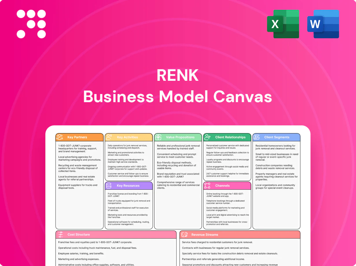
The OmniVision Business Model Canvas previewed here is the actual deliverable, not a mockup or sample. After purchase you’ll receive this exact file—complete, editable, and formatted—ready for presentation and strategic use. The same document will be provided as downloadable Word and Excel files.

Business Model Canvas: Strategic Blueprint to Create Value and Capture Revenue
Unlock the strategic blueprint behind OmniVision with our Business Model Canvas—3–5 concise, actionable sentences that reveal how the company creates value, captures revenue, and sustains competitive advantage. Ideal for investors, founders, and analysts seeking a clear playbook. Download the full Word/Excel canvas to benchmark, adapt, and execute.
Partnerships
Foundry and OSAT alliances
Partnerships with leading fabs and OSATs secure capacity at advanced nodes, leveraging TSMC's ~56% global foundry share in 2024 and a global OSAT market ~26 billion USD in 2024 to support competitive yields. These alliances enable pixel innovations such as stacked and BSI sensors and close DFM and test collaboration that shortens time-to-yield. Multi-sourcing across multiple fabs and OSATs mitigates supply risk and cost volatility.
OEMs and Tier-1 system integrators
Co-development with smartphone, automotive, and security OEMs aligns OmniVision roadmaps to end-market needs, enabling tailored sensor features and ISP tuning. Early engagement secures design wins and ramps, often converting into multi-year programs that drive unit volumes. Joint validation shortens qualification cycles, cutting time-to-production by months. Long-term agreements stabilize volumes and pricing in volatile markets (automotive camera market >$8.6B in 2024).
Module makers and EMS partners
Camera module partners integrate OmniVision sensors, lenses and ISPs into turnkey units that in 2024 shipped in hundreds of millions of devices globally. EMS firms compress NPI to mass production from months to weeks, enabling faster ramp across tiers. Shared FA/QA processes across partners improve reliability and reduce field failures, accelerating scale from entry to flagship devices.
EDA, IP, and semiconductor ecosystem
OmniVision leverages tight relationships with EDA vendors, sensor IP providers, and substrate suppliers (including foundry PDK access such as TSMC nodes) to accelerate sensor-to-silicon design, improve performance and area, and shorten time-to-market. Joint reference flows and shared verification libraries cut respin risk and yield cycles, while active standards participation ensures device and interface interoperability across the semiconductor ecosystem.
Universities and research institutes
- 2024 partnerships: joint labs and sponsored projects
- Outputs: patentable research and prototypes
- Talent: direct recruiting pipelines for imaging, AI, materials
- Risk: shared labs reduce early technical risk
Strategic fabs/OSATs secure advanced-node capacity; co-development with OEMs speeds multi-year ramps
Strategic fabs/OSATs (TSMC ~56% share; global OSAT market ~$26B in 2024) secure advanced-node capacity and yield. Co-development with smartphone, automotive (> $8.6B camera market 2024) and security OEMs drives multi-year design wins and faster ramps. University and IP partners supply patents, prototypes and talent, shortening validation and reducing respin risk.
| Partnership | Key partners | 2024 metric |
|---|---|---|
| Foundry/OSAT | TSMC, major OSATs | TSMC ~56% share; OSAT ~$26B |
| OEMs | Smartphone, Automotive | Auto camera >$8.6B |
| Research/IP | Universities, EDA | Joint labs, patents |
What is included in the product
Detailed Word Document
A comprehensive, pre-written Business Model Canvas for OmniVision covering all nine BMC blocks—customer segments, value propositions, channels, customer relationships, revenue streams, key resources, key activities, key partnerships, and cost structure—aligned with real-world operations and strategy; includes SWOT-linked competitive analysis and a polished, presentation-ready format for investors and internal planning.
Customizable Excel Spreadsheet
High-level, editable one-page snapshot that condenses OmniVision’s strategy and relieves the pain of lengthy reports—saving hours of formatting while enabling quick comparisons, team collaboration, and fast executive deliverables.
Activities
Sensor and ISP R&D
Designing advanced CMOS image sensors with stacked pixels and on-sensor processing is core, targeting markets where CMOS holds over 90% share and the global image sensor market was roughly $20 billion in 2024. Algorithm development focuses on HDR, low-light enhancement and noise reduction to meet mobile and automotive specs. Teams continuously optimize power, area and performance trade-offs and run benchmarking programs to sustain leadership.
System and module co-design
Co-design of sensors with lenses, ISPs and firmware ensures end-to-end image quality and system-level performance; OmniVision in 2024 emphasized this integration to improve image pipelines and reduce field issues. Reference designs accelerate customer integration and shorten design-in cycles. Early thermal and EMI engineering prevents late-stage reruns. Rapid prototyping supports fast design-ins.
Quality, reliability, and certification
Automotive AEC-Q100, medical and industrial standards mandate rigorous testing across product lifecycles; burn-in and HTOL are standard stress tests and functional safety documentation supports ISO 26262 compliance. Traceability is maintained via serial lot data and PPAPs (levels 1–5) to support IATF 16949 audits. Field reliability data is closed-looped into design revisions to reduce warranty exposure and improve failure rates.
Supply chain and operations management
In 2024 OmniVision orchestrated wafer starts, packaging, and final test across foundry and OSAT partners to meet customer roadmaps while running continuous yield-improvement and cost-down programs.
Inventory and demand planning balance multi-week lead times across wafers and packages, and risk management covers critical materials, freight, and dual-sourcing strategies to mitigate disruptions.
- Wafer starts coordinated with partners
- Ongoing yield and cost-down programs
- Inventory vs demand planning for lead-time balance
- Material, logistics, and dual-source risk management
Go-to-market and customer enablement
Design-win pursuit with FAEs and solution marketing drives revenue by aligning sensor solutions to OEM roadmaps; SDKs, drivers and reference software cut customer integration effort and time to market. Application notes and eval kits enable rapid validation, while structured post-sales support sustains relationships and repeat business.
- Design-win focus with FAEs
- SDKs and drivers reduce integration effort
- Reference software and eval kits for validation
- Post-sales support for retention
Stacked-pixel CMOS sensors with on-sensor processing for a $20B market
OmniVision designs advanced CMOS image sensors with stacked pixels and on-sensor processing, targeting a global image sensor market of about $20 billion in 2024 where CMOS holds >90% share. Algorithm work centers on HDR, low-light and noise reduction; teams run power/area/perf optimizations and benchmarking. Manufacturing orchestration with foundries/OSATs manages wafer starts, packaging and multi-week lead times. Design-win efforts use FAEs, SDKs, eval kits and post-sales support.
| Metric | 2024 |
|---|---|
| Global image sensor market | $20B |
| CMOS market share | >90% |
| PPAP levels | 1–5 |
| Lead times | Multi-week |
Full Document Unlocks After Purchase
Business Model Canvas
The OmniVision Business Model Canvas previewed here is the actual deliverable, not a mockup or sample. After purchase you’ll receive this exact file—complete, editable, and formatted—ready for presentation and strategic use. The same document will be provided as downloadable Word and Excel files.
Original: $10.00
-65%$10.00
$3.50Description
Business Model Canvas: Strategic Blueprint to Create Value and Capture Revenue
Unlock the strategic blueprint behind OmniVision with our Business Model Canvas—3–5 concise, actionable sentences that reveal how the company creates value, captures revenue, and sustains competitive advantage. Ideal for investors, founders, and analysts seeking a clear playbook. Download the full Word/Excel canvas to benchmark, adapt, and execute.
Partnerships
Foundry and OSAT alliances
Partnerships with leading fabs and OSATs secure capacity at advanced nodes, leveraging TSMC's ~56% global foundry share in 2024 and a global OSAT market ~26 billion USD in 2024 to support competitive yields. These alliances enable pixel innovations such as stacked and BSI sensors and close DFM and test collaboration that shortens time-to-yield. Multi-sourcing across multiple fabs and OSATs mitigates supply risk and cost volatility.
OEMs and Tier-1 system integrators
Co-development with smartphone, automotive, and security OEMs aligns OmniVision roadmaps to end-market needs, enabling tailored sensor features and ISP tuning. Early engagement secures design wins and ramps, often converting into multi-year programs that drive unit volumes. Joint validation shortens qualification cycles, cutting time-to-production by months. Long-term agreements stabilize volumes and pricing in volatile markets (automotive camera market >$8.6B in 2024).
Module makers and EMS partners
Camera module partners integrate OmniVision sensors, lenses and ISPs into turnkey units that in 2024 shipped in hundreds of millions of devices globally. EMS firms compress NPI to mass production from months to weeks, enabling faster ramp across tiers. Shared FA/QA processes across partners improve reliability and reduce field failures, accelerating scale from entry to flagship devices.
EDA, IP, and semiconductor ecosystem
OmniVision leverages tight relationships with EDA vendors, sensor IP providers, and substrate suppliers (including foundry PDK access such as TSMC nodes) to accelerate sensor-to-silicon design, improve performance and area, and shorten time-to-market. Joint reference flows and shared verification libraries cut respin risk and yield cycles, while active standards participation ensures device and interface interoperability across the semiconductor ecosystem.
Universities and research institutes
- 2024 partnerships: joint labs and sponsored projects
- Outputs: patentable research and prototypes
- Talent: direct recruiting pipelines for imaging, AI, materials
- Risk: shared labs reduce early technical risk
Strategic fabs/OSATs secure advanced-node capacity; co-development with OEMs speeds multi-year ramps
Strategic fabs/OSATs (TSMC ~56% share; global OSAT market ~$26B in 2024) secure advanced-node capacity and yield. Co-development with smartphone, automotive (> $8.6B camera market 2024) and security OEMs drives multi-year design wins and faster ramps. University and IP partners supply patents, prototypes and talent, shortening validation and reducing respin risk.
| Partnership | Key partners | 2024 metric |
|---|---|---|
| Foundry/OSAT | TSMC, major OSATs | TSMC ~56% share; OSAT ~$26B |
| OEMs | Smartphone, Automotive | Auto camera >$8.6B |
| Research/IP | Universities, EDA | Joint labs, patents |
What is included in the product
Detailed Word Document
A comprehensive, pre-written Business Model Canvas for OmniVision covering all nine BMC blocks—customer segments, value propositions, channels, customer relationships, revenue streams, key resources, key activities, key partnerships, and cost structure—aligned with real-world operations and strategy; includes SWOT-linked competitive analysis and a polished, presentation-ready format for investors and internal planning.
Customizable Excel Spreadsheet
High-level, editable one-page snapshot that condenses OmniVision’s strategy and relieves the pain of lengthy reports—saving hours of formatting while enabling quick comparisons, team collaboration, and fast executive deliverables.
Activities
Sensor and ISP R&D
Designing advanced CMOS image sensors with stacked pixels and on-sensor processing is core, targeting markets where CMOS holds over 90% share and the global image sensor market was roughly $20 billion in 2024. Algorithm development focuses on HDR, low-light enhancement and noise reduction to meet mobile and automotive specs. Teams continuously optimize power, area and performance trade-offs and run benchmarking programs to sustain leadership.
System and module co-design
Co-design of sensors with lenses, ISPs and firmware ensures end-to-end image quality and system-level performance; OmniVision in 2024 emphasized this integration to improve image pipelines and reduce field issues. Reference designs accelerate customer integration and shorten design-in cycles. Early thermal and EMI engineering prevents late-stage reruns. Rapid prototyping supports fast design-ins.
Quality, reliability, and certification
Automotive AEC-Q100, medical and industrial standards mandate rigorous testing across product lifecycles; burn-in and HTOL are standard stress tests and functional safety documentation supports ISO 26262 compliance. Traceability is maintained via serial lot data and PPAPs (levels 1–5) to support IATF 16949 audits. Field reliability data is closed-looped into design revisions to reduce warranty exposure and improve failure rates.
Supply chain and operations management
In 2024 OmniVision orchestrated wafer starts, packaging, and final test across foundry and OSAT partners to meet customer roadmaps while running continuous yield-improvement and cost-down programs.
Inventory and demand planning balance multi-week lead times across wafers and packages, and risk management covers critical materials, freight, and dual-sourcing strategies to mitigate disruptions.
- Wafer starts coordinated with partners
- Ongoing yield and cost-down programs
- Inventory vs demand planning for lead-time balance
- Material, logistics, and dual-source risk management
Go-to-market and customer enablement
Design-win pursuit with FAEs and solution marketing drives revenue by aligning sensor solutions to OEM roadmaps; SDKs, drivers and reference software cut customer integration effort and time to market. Application notes and eval kits enable rapid validation, while structured post-sales support sustains relationships and repeat business.
- Design-win focus with FAEs
- SDKs and drivers reduce integration effort
- Reference software and eval kits for validation
- Post-sales support for retention
Stacked-pixel CMOS sensors with on-sensor processing for a $20B market
OmniVision designs advanced CMOS image sensors with stacked pixels and on-sensor processing, targeting a global image sensor market of about $20 billion in 2024 where CMOS holds >90% share. Algorithm work centers on HDR, low-light and noise reduction; teams run power/area/perf optimizations and benchmarking. Manufacturing orchestration with foundries/OSATs manages wafer starts, packaging and multi-week lead times. Design-win efforts use FAEs, SDKs, eval kits and post-sales support.
| Metric | 2024 |
|---|---|
| Global image sensor market | $20B |
| CMOS market share | >90% |
| PPAP levels | 1–5 |
| Lead times | Multi-week |
Full Document Unlocks After Purchase
Business Model Canvas
The OmniVision Business Model Canvas previewed here is the actual deliverable, not a mockup or sample. After purchase you’ll receive this exact file—complete, editable, and formatted—ready for presentation and strategic use. The same document will be provided as downloadable Word and Excel files.