Semiconductor Manufacturing International Business Model Canvas

Business Model Canvas for Leading Chip Manufacturer: Value, Partners, Revenue
Unlock the full strategic blueprint behind Semiconductor Manufacturing International with our Business Model Canvas—three to five concise sections map value propositions, key partners, revenue streams and cost structure. Ideal for investors, consultants, and entrepreneurs seeking actionable insights. Download the editable Word & Excel files to benchmark, adapt, and drive smarter strategic decisions today.
Partnerships

Equipment and Tool Vendors
Partnerships with lithography, etch, deposition and metrology suppliers (ASML holding >90% of commercial EUV capacity; Applied Materials and Lam Research leading mature-node tools) ensure access to leading toolsets. Joint process qualifications and aligned tool roadmaps cut time-to-yield by up to 25%. Preferred service contracts target uptime >92% and stabilize OEE. Co-investment or volume commitments secure allocations in constrained markets.
Materials and Substrate Suppliers
Strategic ties with wafer suppliers (SUMCO, Shin-Etsu), photoresist vendors (JSR, TOK), gases and specialty chemical providers (Merck) safeguard quality and supply continuity amid heavy 2024 fab investment (TSMC capex $40–44 billion). Multi-sourcing and VMI reduce lead-time risk and inventory strain. Joint SPC and quality audits improve process stability. Long-term agreements stabilize pricing and ensure priority allocation.

EDA, IP, and Design Ecosystem
In 2024 SMIC's alliances with leading EDA and IP providers deliver validated PDKs and reference flows that shorten design cycles and reduce first-pass silicon risk. Pre-qualified libraries, PHYs and RF/IP blocks accelerate customer tape-outs and lower integration cost. Co-marketing of design enablement reduces customer friction and adoption barriers. Continuous model updates improve design-to-silicon correlation and yield predictability.

OSAT and Test Partners
Packaging and test partners extend services beyond wafer fabrication, with the global OSAT market reaching about USD 40B in 2024, enabling turnkey flows that streamline logistics and reduce cycle time for customers. Co-developed reliability and automotive-grade flows conform to AEC-Q100 and ISO 26262 standards, while joint root-cause analysis accelerates time-to-quality during volume ramps.
- Turnkey logistics: single-source wafer-to-board
- Standards: AEC-Q100, ISO 26262
- Market size: ~USD 40B (2024)
- Joint RCA: faster volume qualification
Academic, Consortia, and Government Bodies
Collaboration with universities, consortia and government bodies strengthens workforce pipelines and joint R&D in new materials and devices, leveraging global semiconductor R&D spending near $80B in 2024; participation in consortia accelerates benchmarking and learning; grants such as the US CHIPS Act ($52B) can offset capex and localization; standards work shortens qualification cycles and improves interoperability.
- Workforce/R&D: university partnerships
- Consortia: faster benchmarking
- Grants: $52B CHIPS offsets capex
- Standards: improved qualification efficiency
Equipment and materials partnerships cut time-to-yield ~25% and secure uptime >92%
Partnerships with ASML (>90% commercial EUV), Applied/Lam and material suppliers secure tool access and reduce time-to-yield by ~25%; preferred service contracts target uptime >92% and OEE stability. Long-term wafer/photoresist/gas agreements and co-investments mitigate allocation risk amid TSMC capex $40–44B (2024). University/consortia links and CHIPS $52B grants support R&D (~$80B global 2024) and workforce.
| Partner | Metric (2024) |
|---|---|
| ASML | >90% EUV |
| TSMC capex | $40–44B |
| OSAT | ~$40B |
| CHIPS | $52B |
What is included in the product
 Detailed Word Document
A concise, pre-built Business Model Canvas for Semiconductor Manufacturing International (SMIC) detailing customer segments, value propositions, channels, revenue streams and key partners aligned to fab operations and technology roadmap. Ideal for investor presentations, strategic planning and competitive analysis with linked SWOT insights and operational KPIs across the nine BMC blocks.

 Customizable Excel Spreadsheet
High-level view of SMIC's business model with editable cells, condensing fab economics, capacity constraints, supply-chain risks and customer segmentation into a one-page snapshot that saves hours of structuring and accelerates boardroom decisions and scenario planning.
Activities

Process and Technology Development
Develop and refine logic, mixed-signal, RF, power, eNVM and CIS platforms with PDK creation, device modeling and DTCO to align design and process; PDK cadences are commonly 6–12 months. Continuous shrink and module optimization lift performance and cost-efficiency, while qualification to standards such as AEC-Q100 and ISO 26262 (automotive cycles ~18–24 months) enables cross-industry adoption.
Wafer Fabrication and Yield Ramp
High-volume wafer fabrication in 2024 relies on tight SPC and APC to hold process variability within targets that enable ramp-to-volume in roughly 6–12 months. Defect reduction, tool matching and recipe tuning drive yield learning towards mature die yields above 90% at scale. Inline and end-of-line analytics shorten feedback loops, while structured DoE optimizes throughput and wafer cost per good die.

Mask, Tape-Out, and DFM Enablement
Manage tape-out interfaces, OPC/RET and mask logistics including advanced EUV mask blanks that exceed $1M (2024), while supplying DRC/LVS decks, signoff kits and silicon-proven reference flows to accelerate customer qualification. MPW shuttles reduce NRE barriers by enabling low-cost shared runs for prototyping. Tight DFM feedback loops cut re-spins and drive first-pass success, with industry yield uplifts commonly reported in the 10–30% range.

Customer Program Management
Dedicated customer program teams coordinate schedules, risk and engineering change orders, with joint yield taskforces resolving >80% of excursions within 72 hours; NPI gates, PPAP/auto-grade audits and qualification tracking ensure readiness aligned to ISO 9001/IATF standards. Forecasting and capacity planning align fab loads to demand against 2024 foundry market shares (TSMC ~54%, Samsung ~15%).
- Dedicated teams: schedule, ECO, risk
- Yield taskforces: >80% fixes <72h
- Audits: NPI gates, PPAP, auto-grade
- Planning: forecast → fab load alignment (2024 market share cited)
Supply Chain and Facilities Operations
As of 2024 fabs target >95% uptime, so securing materials, critical spares and utilities is central to operations to avoid costly downtime. Energy, water and waste systems are optimized for reliability and ESG compliance. Rigorous preventive maintenance preserves tool availability and performance while business continuity plans mitigate geopolitical and logistics risks.
- Target uptime: >95%
- Spare coverage: critical parts on-hand
- ESG: optimized energy/water/waste systems
- Risk: continuity plans for geopolitical/logistics shocks
PDKs 6–12m; ramp 6–12m; yield >90%; uptime >95%
Platform PDKs: 6–12 months cadence; device modeling and DTCO drive node shrinks. Fab ops: ramp-to-volume 6–12 months, SPC/APC yield learning to >90% mature die yield; uptime targets >95%. Tape-out & masks: EUV mask >$1M (2024), MPW for prototyping; yield uplifts 10–30%, joint taskforces fix >80% excursions within 72h; auto qual 18–24 months.
| Metric | 2024 Value |
|---|---|
| PDK cadence | 6–12 months |
| Ramp-to-volume | 6–12 months |
| Mature die yield | >90% |
| Fab uptime | >95% |
| EUV mask cost | >$1M |
| TSMC market share | ~54% |
Delivered as Displayed
Business Model Canvas
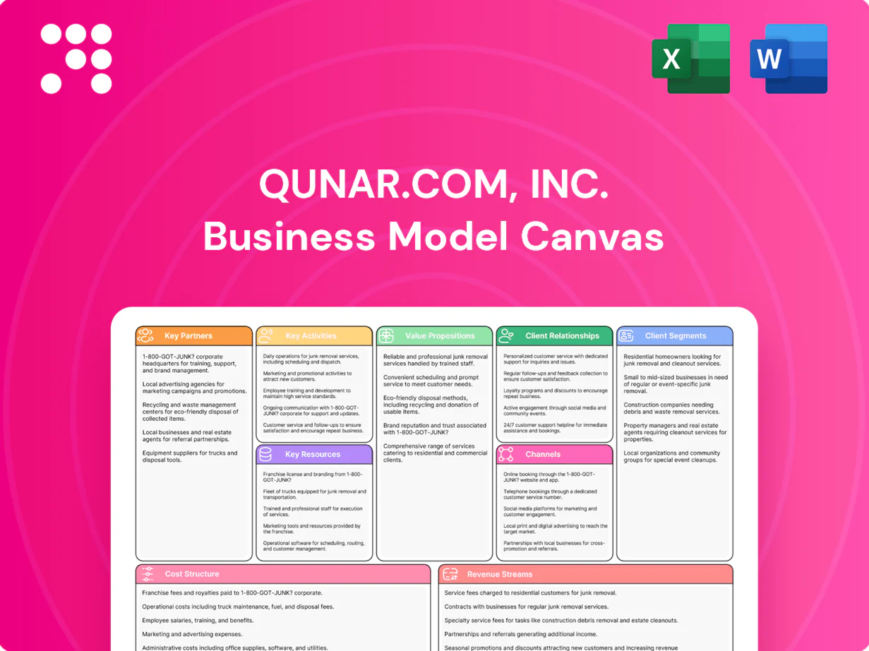
The Semiconductor Manufacturing International Business Model Canvas shown here is the real deliverable, not a mockup. When you purchase, you’ll receive this exact Business Model Canvas file—complete, editable, and formatted for immediate use. No placeholders, no surprises—what you see is what you’ll own.

Business Model Canvas for Leading Chip Manufacturer: Value, Partners, Revenue
Unlock the full strategic blueprint behind Semiconductor Manufacturing International with our Business Model Canvas—three to five concise sections map value propositions, key partners, revenue streams and cost structure. Ideal for investors, consultants, and entrepreneurs seeking actionable insights. Download the editable Word & Excel files to benchmark, adapt, and drive smarter strategic decisions today.
Partnerships
Equipment and Tool Vendors
Partnerships with lithography, etch, deposition and metrology suppliers (ASML holding >90% of commercial EUV capacity; Applied Materials and Lam Research leading mature-node tools) ensure access to leading toolsets. Joint process qualifications and aligned tool roadmaps cut time-to-yield by up to 25%. Preferred service contracts target uptime >92% and stabilize OEE. Co-investment or volume commitments secure allocations in constrained markets.
Materials and Substrate Suppliers
Strategic ties with wafer suppliers (SUMCO, Shin-Etsu), photoresist vendors (JSR, TOK), gases and specialty chemical providers (Merck) safeguard quality and supply continuity amid heavy 2024 fab investment (TSMC capex $40–44 billion). Multi-sourcing and VMI reduce lead-time risk and inventory strain. Joint SPC and quality audits improve process stability. Long-term agreements stabilize pricing and ensure priority allocation.
EDA, IP, and Design Ecosystem
In 2024 SMIC's alliances with leading EDA and IP providers deliver validated PDKs and reference flows that shorten design cycles and reduce first-pass silicon risk. Pre-qualified libraries, PHYs and RF/IP blocks accelerate customer tape-outs and lower integration cost. Co-marketing of design enablement reduces customer friction and adoption barriers. Continuous model updates improve design-to-silicon correlation and yield predictability.
OSAT and Test Partners
Packaging and test partners extend services beyond wafer fabrication, with the global OSAT market reaching about USD 40B in 2024, enabling turnkey flows that streamline logistics and reduce cycle time for customers. Co-developed reliability and automotive-grade flows conform to AEC-Q100 and ISO 26262 standards, while joint root-cause analysis accelerates time-to-quality during volume ramps.
- Turnkey logistics: single-source wafer-to-board
- Standards: AEC-Q100, ISO 26262
- Market size: ~USD 40B (2024)
- Joint RCA: faster volume qualification
Academic, Consortia, and Government Bodies
Collaboration with universities, consortia and government bodies strengthens workforce pipelines and joint R&D in new materials and devices, leveraging global semiconductor R&D spending near $80B in 2024; participation in consortia accelerates benchmarking and learning; grants such as the US CHIPS Act ($52B) can offset capex and localization; standards work shortens qualification cycles and improves interoperability.
- Workforce/R&D: university partnerships
- Consortia: faster benchmarking
- Grants: $52B CHIPS offsets capex
- Standards: improved qualification efficiency
Equipment and materials partnerships cut time-to-yield ~25% and secure uptime >92%
Partnerships with ASML (>90% commercial EUV), Applied/Lam and material suppliers secure tool access and reduce time-to-yield by ~25%; preferred service contracts target uptime >92% and OEE stability. Long-term wafer/photoresist/gas agreements and co-investments mitigate allocation risk amid TSMC capex $40–44B (2024). University/consortia links and CHIPS $52B grants support R&D (~$80B global 2024) and workforce.
| Partner | Metric (2024) |
|---|---|
| ASML | >90% EUV |
| TSMC capex | $40–44B |
| OSAT | ~$40B |
| CHIPS | $52B |
What is included in the product
Detailed Word Document
A concise, pre-built Business Model Canvas for Semiconductor Manufacturing International (SMIC) detailing customer segments, value propositions, channels, revenue streams and key partners aligned to fab operations and technology roadmap. Ideal for investor presentations, strategic planning and competitive analysis with linked SWOT insights and operational KPIs across the nine BMC blocks.
Customizable Excel Spreadsheet
High-level view of SMIC's business model with editable cells, condensing fab economics, capacity constraints, supply-chain risks and customer segmentation into a one-page snapshot that saves hours of structuring and accelerates boardroom decisions and scenario planning.
Activities
Process and Technology Development
Develop and refine logic, mixed-signal, RF, power, eNVM and CIS platforms with PDK creation, device modeling and DTCO to align design and process; PDK cadences are commonly 6–12 months. Continuous shrink and module optimization lift performance and cost-efficiency, while qualification to standards such as AEC-Q100 and ISO 26262 (automotive cycles ~18–24 months) enables cross-industry adoption.
Wafer Fabrication and Yield Ramp
High-volume wafer fabrication in 2024 relies on tight SPC and APC to hold process variability within targets that enable ramp-to-volume in roughly 6–12 months. Defect reduction, tool matching and recipe tuning drive yield learning towards mature die yields above 90% at scale. Inline and end-of-line analytics shorten feedback loops, while structured DoE optimizes throughput and wafer cost per good die.
Mask, Tape-Out, and DFM Enablement
Manage tape-out interfaces, OPC/RET and mask logistics including advanced EUV mask blanks that exceed $1M (2024), while supplying DRC/LVS decks, signoff kits and silicon-proven reference flows to accelerate customer qualification. MPW shuttles reduce NRE barriers by enabling low-cost shared runs for prototyping. Tight DFM feedback loops cut re-spins and drive first-pass success, with industry yield uplifts commonly reported in the 10–30% range.
Customer Program Management
Dedicated customer program teams coordinate schedules, risk and engineering change orders, with joint yield taskforces resolving >80% of excursions within 72 hours; NPI gates, PPAP/auto-grade audits and qualification tracking ensure readiness aligned to ISO 9001/IATF standards. Forecasting and capacity planning align fab loads to demand against 2024 foundry market shares (TSMC ~54%, Samsung ~15%).
- Dedicated teams: schedule, ECO, risk
- Yield taskforces: >80% fixes <72h
- Audits: NPI gates, PPAP, auto-grade
- Planning: forecast → fab load alignment (2024 market share cited)
Supply Chain and Facilities Operations
As of 2024 fabs target >95% uptime, so securing materials, critical spares and utilities is central to operations to avoid costly downtime. Energy, water and waste systems are optimized for reliability and ESG compliance. Rigorous preventive maintenance preserves tool availability and performance while business continuity plans mitigate geopolitical and logistics risks.
- Target uptime: >95%
- Spare coverage: critical parts on-hand
- ESG: optimized energy/water/waste systems
- Risk: continuity plans for geopolitical/logistics shocks
PDKs 6–12m; ramp 6–12m; yield >90%; uptime >95%
Platform PDKs: 6–12 months cadence; device modeling and DTCO drive node shrinks. Fab ops: ramp-to-volume 6–12 months, SPC/APC yield learning to >90% mature die yield; uptime targets >95%. Tape-out & masks: EUV mask >$1M (2024), MPW for prototyping; yield uplifts 10–30%, joint taskforces fix >80% excursions within 72h; auto qual 18–24 months.
| Metric | 2024 Value |
|---|---|
| PDK cadence | 6–12 months |
| Ramp-to-volume | 6–12 months |
| Mature die yield | >90% |
| Fab uptime | >95% |
| EUV mask cost | >$1M |
| TSMC market share | ~54% |
Delivered as Displayed
Business Model Canvas
The Semiconductor Manufacturing International Business Model Canvas shown here is the real deliverable, not a mockup. When you purchase, you’ll receive this exact Business Model Canvas file—complete, editable, and formatted for immediate use. No placeholders, no surprises—what you see is what you’ll own.
Description
Business Model Canvas for Leading Chip Manufacturer: Value, Partners, Revenue
Unlock the full strategic blueprint behind Semiconductor Manufacturing International with our Business Model Canvas—three to five concise sections map value propositions, key partners, revenue streams and cost structure. Ideal for investors, consultants, and entrepreneurs seeking actionable insights. Download the editable Word & Excel files to benchmark, adapt, and drive smarter strategic decisions today.
Partnerships
Equipment and Tool Vendors
Partnerships with lithography, etch, deposition and metrology suppliers (ASML holding >90% of commercial EUV capacity; Applied Materials and Lam Research leading mature-node tools) ensure access to leading toolsets. Joint process qualifications and aligned tool roadmaps cut time-to-yield by up to 25%. Preferred service contracts target uptime >92% and stabilize OEE. Co-investment or volume commitments secure allocations in constrained markets.
Materials and Substrate Suppliers
Strategic ties with wafer suppliers (SUMCO, Shin-Etsu), photoresist vendors (JSR, TOK), gases and specialty chemical providers (Merck) safeguard quality and supply continuity amid heavy 2024 fab investment (TSMC capex $40–44 billion). Multi-sourcing and VMI reduce lead-time risk and inventory strain. Joint SPC and quality audits improve process stability. Long-term agreements stabilize pricing and ensure priority allocation.
EDA, IP, and Design Ecosystem
In 2024 SMIC's alliances with leading EDA and IP providers deliver validated PDKs and reference flows that shorten design cycles and reduce first-pass silicon risk. Pre-qualified libraries, PHYs and RF/IP blocks accelerate customer tape-outs and lower integration cost. Co-marketing of design enablement reduces customer friction and adoption barriers. Continuous model updates improve design-to-silicon correlation and yield predictability.
OSAT and Test Partners
Packaging and test partners extend services beyond wafer fabrication, with the global OSAT market reaching about USD 40B in 2024, enabling turnkey flows that streamline logistics and reduce cycle time for customers. Co-developed reliability and automotive-grade flows conform to AEC-Q100 and ISO 26262 standards, while joint root-cause analysis accelerates time-to-quality during volume ramps.
- Turnkey logistics: single-source wafer-to-board
- Standards: AEC-Q100, ISO 26262
- Market size: ~USD 40B (2024)
- Joint RCA: faster volume qualification
Academic, Consortia, and Government Bodies
Collaboration with universities, consortia and government bodies strengthens workforce pipelines and joint R&D in new materials and devices, leveraging global semiconductor R&D spending near $80B in 2024; participation in consortia accelerates benchmarking and learning; grants such as the US CHIPS Act ($52B) can offset capex and localization; standards work shortens qualification cycles and improves interoperability.
- Workforce/R&D: university partnerships
- Consortia: faster benchmarking
- Grants: $52B CHIPS offsets capex
- Standards: improved qualification efficiency
Equipment and materials partnerships cut time-to-yield ~25% and secure uptime >92%
Partnerships with ASML (>90% commercial EUV), Applied/Lam and material suppliers secure tool access and reduce time-to-yield by ~25%; preferred service contracts target uptime >92% and OEE stability. Long-term wafer/photoresist/gas agreements and co-investments mitigate allocation risk amid TSMC capex $40–44B (2024). University/consortia links and CHIPS $52B grants support R&D (~$80B global 2024) and workforce.
| Partner | Metric (2024) |
|---|---|
| ASML | >90% EUV |
| TSMC capex | $40–44B |
| OSAT | ~$40B |
| CHIPS | $52B |
What is included in the product
Detailed Word Document
A concise, pre-built Business Model Canvas for Semiconductor Manufacturing International (SMIC) detailing customer segments, value propositions, channels, revenue streams and key partners aligned to fab operations and technology roadmap. Ideal for investor presentations, strategic planning and competitive analysis with linked SWOT insights and operational KPIs across the nine BMC blocks.
Customizable Excel Spreadsheet
High-level view of SMIC's business model with editable cells, condensing fab economics, capacity constraints, supply-chain risks and customer segmentation into a one-page snapshot that saves hours of structuring and accelerates boardroom decisions and scenario planning.
Activities
Process and Technology Development
Develop and refine logic, mixed-signal, RF, power, eNVM and CIS platforms with PDK creation, device modeling and DTCO to align design and process; PDK cadences are commonly 6–12 months. Continuous shrink and module optimization lift performance and cost-efficiency, while qualification to standards such as AEC-Q100 and ISO 26262 (automotive cycles ~18–24 months) enables cross-industry adoption.
Wafer Fabrication and Yield Ramp
High-volume wafer fabrication in 2024 relies on tight SPC and APC to hold process variability within targets that enable ramp-to-volume in roughly 6–12 months. Defect reduction, tool matching and recipe tuning drive yield learning towards mature die yields above 90% at scale. Inline and end-of-line analytics shorten feedback loops, while structured DoE optimizes throughput and wafer cost per good die.
Mask, Tape-Out, and DFM Enablement
Manage tape-out interfaces, OPC/RET and mask logistics including advanced EUV mask blanks that exceed $1M (2024), while supplying DRC/LVS decks, signoff kits and silicon-proven reference flows to accelerate customer qualification. MPW shuttles reduce NRE barriers by enabling low-cost shared runs for prototyping. Tight DFM feedback loops cut re-spins and drive first-pass success, with industry yield uplifts commonly reported in the 10–30% range.
Customer Program Management
Dedicated customer program teams coordinate schedules, risk and engineering change orders, with joint yield taskforces resolving >80% of excursions within 72 hours; NPI gates, PPAP/auto-grade audits and qualification tracking ensure readiness aligned to ISO 9001/IATF standards. Forecasting and capacity planning align fab loads to demand against 2024 foundry market shares (TSMC ~54%, Samsung ~15%).
- Dedicated teams: schedule, ECO, risk
- Yield taskforces: >80% fixes <72h
- Audits: NPI gates, PPAP, auto-grade
- Planning: forecast → fab load alignment (2024 market share cited)
Supply Chain and Facilities Operations
As of 2024 fabs target >95% uptime, so securing materials, critical spares and utilities is central to operations to avoid costly downtime. Energy, water and waste systems are optimized for reliability and ESG compliance. Rigorous preventive maintenance preserves tool availability and performance while business continuity plans mitigate geopolitical and logistics risks.
- Target uptime: >95%
- Spare coverage: critical parts on-hand
- ESG: optimized energy/water/waste systems
- Risk: continuity plans for geopolitical/logistics shocks
PDKs 6–12m; ramp 6–12m; yield >90%; uptime >95%
Platform PDKs: 6–12 months cadence; device modeling and DTCO drive node shrinks. Fab ops: ramp-to-volume 6–12 months, SPC/APC yield learning to >90% mature die yield; uptime targets >95%. Tape-out & masks: EUV mask >$1M (2024), MPW for prototyping; yield uplifts 10–30%, joint taskforces fix >80% excursions within 72h; auto qual 18–24 months.
| Metric | 2024 Value |
|---|---|
| PDK cadence | 6–12 months |
| Ramp-to-volume | 6–12 months |
| Mature die yield | >90% |
| Fab uptime | >95% |
| EUV mask cost | >$1M |
| TSMC market share | ~54% |
Delivered as Displayed
Business Model Canvas
The Semiconductor Manufacturing International Business Model Canvas shown here is the real deliverable, not a mockup. When you purchase, you’ll receive this exact Business Model Canvas file—complete, editable, and formatted for immediate use. No placeholders, no surprises—what you see is what you’ll own.