VIS Business Model Canvas

Unlock a concise Business Model Canvas preview that maps value, customers, and revenue
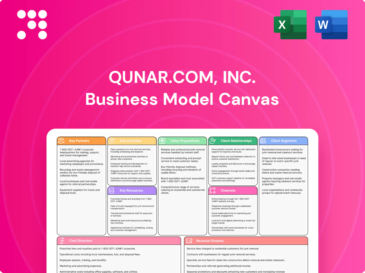
Unlock VIS’s strategic playbook with our concise Business Model Canvas preview—designed to show how value, customers, and revenue interlock to drive growth. Dive into the full Canvas for a complete, section-by-section breakdown with actionable insights and financial implications. Purchase the downloadable Word and Excel files to benchmark, adapt, and scale your strategy today.
Partnerships

Wafer equipment and materials suppliers
Strategic ties with lithography, etch, deposition and test vendors secure leading toolsets and fast spares; ASML remains the sole supplier of EUV systems in 2024. Long-term contracts with top wafer suppliers Shin‑Etsu and SUMCO and specialty gas/photoresist vendors stabilize input quality and pricing. Co-development tailors tools for HV, mixed‑signal and analog nodes, while joint roadmaps with suppliers shorten cycle times and improve yield.
IP licensors and EDA ecosystem
Alliances with IP vendors for analog, memory macros and interface blocks accelerate customer tape-outs and reuse proven building blocks; partnerships with EDA firms (Big Three held >80% share in 2023–24) secure robust PDKs, POC flows and design enablement for VIS processes. Reference flows and verification kits cut re-spins, and joint support centers can shorten design-to-silicon timelines materially, improving time-to-market.

OSAT and packaging partners
Collaboration with OSAT and advanced packaging houses delivers turnkey assembly, test and packaging services and in 2024 co-qualification covered five package families: QFN, QFP, BGA, WLCSP and power packages aligned to HV and discrete lines. Shared reliability data and joint test-program development increased final yield by 4–6 percentage points in 2024. Logistics integration shortened cycle times by about 15% and boosted on-time delivery to roughly 98% in 2024.

Key customers as strategic collaborators
Anchor customers in communications, consumer and computing co-invest in process tweaks and capacity reservations, with 2024 early-access pilots funding tooling and layout changes to speed node readiness. Early-access programs steer VIS node evolution through iterative feedback loops and defined KPIs. Joint yield-ramp teams shorten NPI stabilization cycles, and multi-year agreements enable predictable loading and capex planning.
- Anchor accounts co-invest in pilots and capacity reservations
- 2024 early-access programs guide node roadmaps
- Joint yield-ramp teams accelerate NPI stability
- Multi-year agreements underpin predictable loading and capex
Academia and R&D institutes
Research ties with universities and R&D institutes support device modeling, reliability, and novel materials, with US academic R&D funding remaining above $90 billion in 2024, enabling large-scale sponsored projects targeting HV reliability, analog precision, and embedded memory. Sponsored collaborations commonly fund multi-year projects that shorten time-to-prototype and leverage shared labs to de-risk exploratory technologies while building a robust talent pipeline. Talent pipelines deliver 30–50% of new engineering hires in VIS-focused firms, reinforcing depth in device physics and circuit design.
- Research focus: device modeling, reliability, new materials
- Sponsored projects: HV reliability, analog precision, embedded memory
- Shared labs: lower prototype cost and technical risk
- Talent pipeline: significant source of engineering hires
Supplier, EDA and OSAT alliances boost yield +4–6 pts, cut cycle ≈15%, 98% OT
Strategic supplier and IP/EDA alliances (ASML sole EUV 2024; Big Three EDA >80% 2023–24) secure tools, PDKs and co-development, stabilizing inputs via Shin‑Etsu/SUMCO. OSAT/pack partners co-qualify five package families, lifting final yield +4–6 pts and cutting cycle time ≈15% (on-time delivery ~98% in 2024). University and anchor-customer collaborations fund pilots, supplying 30–50% of new hires and leveraging >$90B US academic R&D in 2024.
| Partner | 2024 metric | Impact |
|---|---|---|
| ASML | sole EUV supplier | node enablement |
| Big Three EDA | >80% share | PDKs & flows |
| OSAT | 5 packages co-qualified | +4–6% yield, 98% OT |
| Academia | >$90B US R&D | 30–50% hires, sponsored R&D |
What is included in the product
 Detailed Word Document
A concise, pre-written VIS Business Model Canvas mapping nine classic BMC blocks to the company’s strategy, value propositions, channels and customer segments with narrative and competitive insights. Ideal for presentations, funding discussions and data-driven validation of business ideas.

 Customizable Excel Spreadsheet
High-level view of the VIS Business Model Canvas with editable cells that relieves the pain of scattered strategy notes and unclear responsibilities. Saves hours of formatting by delivering a clean, shareable one-page snapshot ideal for fast decision-making and collaborative iteration.
Activities

Specialty process development
Continuous refinement of HV, mixed-signal, analog, discrete and specialty memory nodes, driven by device modeling and quarterly PDK updates, expands SPICE corner coverage to industry-standard 27 corners. Reliability qualification follows AEC-Q100 and ISO 26262 (up to ASIL D) for automotive, industrial and consumer. DOE cycles (typically 3–5 factor designs) iterate to enhance performance and reduce cost.
High-yield wafer fabrication
Operate fabs with strict SPC, APC and full traceability, achieving wafer-level yields of 88-96% in advanced-node 2024 benchmarks. Inline metrology and feedback control cut parametric variation ~30% and tighten CD sigma to ~2–3 nm. Defect reduction and recipe optimization pushed defect density <0.1/cm2 and raised throughput 10–18%, enabling capacity balancing to meet customer lead times of 6–12 weeks.

Design enablement and tape-out support
Provide validated PDKs, DRC/LVS decks and analog-focused reference flows and run detailed design reviews and mask-data prep to compress time-to-silicon to 12–20 weeks. Offer MPW/shuttle prototyping (reducing NRE by ~60–80% versus full-flow runs) and coordinate seamlessly with foundries (TSMC, Samsung, GlobalFoundries) and EDA/IP partners (Cadence, Synopsys, Arm) for handoff and IP integration.

Quality, reliability, and compliance
Execute qualification plans (HTOL, HAST, ESD/LU) aligned to ISO 9001 and IATF 16949 requirements, with formal test protocols and traceable records. Maintain applicable certifications and participate in customer audits, driving scorecard targets through measurable KPIs. Use 8D root-cause analysis and closed-loop corrective actions to reduce recurrence and improve reliability.
- HTOL/HAST/ESD/LU test execution
- ISO 9001 / IATF 16949 maintenance
- 8D root-cause & corrective actions
- Customer audits & scorecard management
Supply chain and customer program management
Supply chain and customer program management drives forecasting, material planning, and die bank strategies to hit 2024 targets: 95% on-time in-full and cycle times under 8 weeks, with die banks sized for 8–12 week buffers; NPI ramps are managed to reach volume in 12–16 weeks while phase-in/phase-out controls limit disruptions. Cost and yield reporting is updated weekly with action plans reducing scrap/yield loss by targeted 10% year-over-year.
- Forecasting: rolling 12-week accuracy goal 95%
- Material planning: 8–12 week buffer
- Cycle time: <8 weeks target
- NPI ramp: 12–16 weeks to volume
- Cost/yield: weekly reports, −10% Y/Y scrap
Refine HV/mixed-signal nodes: 12–20 wks to silicon, 95% OTIF
Refine HV/mixed-signal/analog nodes with quarterly PDKs (27 SPICE corners) and DOE cycles (3–5 factors) to meet AEC-Q100/ISO 26262 ASIL D. Operate fabs with SPC/APC achieving 2024 wafer yields 88–96%, CD sigma 2–3 nm, defect density <0.1/cm2. Provide PDKs/MPW, compress time-to-silicon to 12–20 weeks and maintain OTIF 95% with cycle times <8 weeks.
| Metric | 2024 |
|---|---|
| Wafer yield | 88–96% |
| CD sigma | 2–3 nm |
| Defect density | <0.1/cm2 |
| Time-to-silicon | 12–20 wks |
| OTIF | 95% |
Full Document Unlocks After Purchase
Business Model Canvas
The VIS Business Model Canvas you see here is a live preview of the exact document you'll receive—no mockup or sample. After purchase you'll download the full, editable file formatted just as shown. It's ready to edit, present, and apply immediately.

Unlock a concise Business Model Canvas preview that maps value, customers, and revenue
Unlock VIS’s strategic playbook with our concise Business Model Canvas preview—designed to show how value, customers, and revenue interlock to drive growth. Dive into the full Canvas for a complete, section-by-section breakdown with actionable insights and financial implications. Purchase the downloadable Word and Excel files to benchmark, adapt, and scale your strategy today.
Partnerships
Wafer equipment and materials suppliers
Strategic ties with lithography, etch, deposition and test vendors secure leading toolsets and fast spares; ASML remains the sole supplier of EUV systems in 2024. Long-term contracts with top wafer suppliers Shin‑Etsu and SUMCO and specialty gas/photoresist vendors stabilize input quality and pricing. Co-development tailors tools for HV, mixed‑signal and analog nodes, while joint roadmaps with suppliers shorten cycle times and improve yield.
IP licensors and EDA ecosystem
Alliances with IP vendors for analog, memory macros and interface blocks accelerate customer tape-outs and reuse proven building blocks; partnerships with EDA firms (Big Three held >80% share in 2023–24) secure robust PDKs, POC flows and design enablement for VIS processes. Reference flows and verification kits cut re-spins, and joint support centers can shorten design-to-silicon timelines materially, improving time-to-market.
OSAT and packaging partners
Collaboration with OSAT and advanced packaging houses delivers turnkey assembly, test and packaging services and in 2024 co-qualification covered five package families: QFN, QFP, BGA, WLCSP and power packages aligned to HV and discrete lines. Shared reliability data and joint test-program development increased final yield by 4–6 percentage points in 2024. Logistics integration shortened cycle times by about 15% and boosted on-time delivery to roughly 98% in 2024.
Key customers as strategic collaborators
Anchor customers in communications, consumer and computing co-invest in process tweaks and capacity reservations, with 2024 early-access pilots funding tooling and layout changes to speed node readiness. Early-access programs steer VIS node evolution through iterative feedback loops and defined KPIs. Joint yield-ramp teams shorten NPI stabilization cycles, and multi-year agreements enable predictable loading and capex planning.
- Anchor accounts co-invest in pilots and capacity reservations
- 2024 early-access programs guide node roadmaps
- Joint yield-ramp teams accelerate NPI stability
- Multi-year agreements underpin predictable loading and capex
Academia and R&D institutes
Research ties with universities and R&D institutes support device modeling, reliability, and novel materials, with US academic R&D funding remaining above $90 billion in 2024, enabling large-scale sponsored projects targeting HV reliability, analog precision, and embedded memory. Sponsored collaborations commonly fund multi-year projects that shorten time-to-prototype and leverage shared labs to de-risk exploratory technologies while building a robust talent pipeline. Talent pipelines deliver 30–50% of new engineering hires in VIS-focused firms, reinforcing depth in device physics and circuit design.
- Research focus: device modeling, reliability, new materials
- Sponsored projects: HV reliability, analog precision, embedded memory
- Shared labs: lower prototype cost and technical risk
- Talent pipeline: significant source of engineering hires
Supplier, EDA and OSAT alliances boost yield +4–6 pts, cut cycle ≈15%, 98% OT
Strategic supplier and IP/EDA alliances (ASML sole EUV 2024; Big Three EDA >80% 2023–24) secure tools, PDKs and co-development, stabilizing inputs via Shin‑Etsu/SUMCO. OSAT/pack partners co-qualify five package families, lifting final yield +4–6 pts and cutting cycle time ≈15% (on-time delivery ~98% in 2024). University and anchor-customer collaborations fund pilots, supplying 30–50% of new hires and leveraging >$90B US academic R&D in 2024.
| Partner | 2024 metric | Impact |
|---|---|---|
| ASML | sole EUV supplier | node enablement |
| Big Three EDA | >80% share | PDKs & flows |
| OSAT | 5 packages co-qualified | +4–6% yield, 98% OT |
| Academia | >$90B US R&D | 30–50% hires, sponsored R&D |
What is included in the product
Detailed Word Document
A concise, pre-written VIS Business Model Canvas mapping nine classic BMC blocks to the company’s strategy, value propositions, channels and customer segments with narrative and competitive insights. Ideal for presentations, funding discussions and data-driven validation of business ideas.
Customizable Excel Spreadsheet
High-level view of the VIS Business Model Canvas with editable cells that relieves the pain of scattered strategy notes and unclear responsibilities. Saves hours of formatting by delivering a clean, shareable one-page snapshot ideal for fast decision-making and collaborative iteration.
Activities
Specialty process development
Continuous refinement of HV, mixed-signal, analog, discrete and specialty memory nodes, driven by device modeling and quarterly PDK updates, expands SPICE corner coverage to industry-standard 27 corners. Reliability qualification follows AEC-Q100 and ISO 26262 (up to ASIL D) for automotive, industrial and consumer. DOE cycles (typically 3–5 factor designs) iterate to enhance performance and reduce cost.
High-yield wafer fabrication
Operate fabs with strict SPC, APC and full traceability, achieving wafer-level yields of 88-96% in advanced-node 2024 benchmarks. Inline metrology and feedback control cut parametric variation ~30% and tighten CD sigma to ~2–3 nm. Defect reduction and recipe optimization pushed defect density <0.1/cm2 and raised throughput 10–18%, enabling capacity balancing to meet customer lead times of 6–12 weeks.
Design enablement and tape-out support
Provide validated PDKs, DRC/LVS decks and analog-focused reference flows and run detailed design reviews and mask-data prep to compress time-to-silicon to 12–20 weeks. Offer MPW/shuttle prototyping (reducing NRE by ~60–80% versus full-flow runs) and coordinate seamlessly with foundries (TSMC, Samsung, GlobalFoundries) and EDA/IP partners (Cadence, Synopsys, Arm) for handoff and IP integration.
Quality, reliability, and compliance
Execute qualification plans (HTOL, HAST, ESD/LU) aligned to ISO 9001 and IATF 16949 requirements, with formal test protocols and traceable records. Maintain applicable certifications and participate in customer audits, driving scorecard targets through measurable KPIs. Use 8D root-cause analysis and closed-loop corrective actions to reduce recurrence and improve reliability.
- HTOL/HAST/ESD/LU test execution
- ISO 9001 / IATF 16949 maintenance
- 8D root-cause & corrective actions
- Customer audits & scorecard management
Supply chain and customer program management
Supply chain and customer program management drives forecasting, material planning, and die bank strategies to hit 2024 targets: 95% on-time in-full and cycle times under 8 weeks, with die banks sized for 8–12 week buffers; NPI ramps are managed to reach volume in 12–16 weeks while phase-in/phase-out controls limit disruptions. Cost and yield reporting is updated weekly with action plans reducing scrap/yield loss by targeted 10% year-over-year.
- Forecasting: rolling 12-week accuracy goal 95%
- Material planning: 8–12 week buffer
- Cycle time: <8 weeks target
- NPI ramp: 12–16 weeks to volume
- Cost/yield: weekly reports, −10% Y/Y scrap
Refine HV/mixed-signal nodes: 12–20 wks to silicon, 95% OTIF
Refine HV/mixed-signal/analog nodes with quarterly PDKs (27 SPICE corners) and DOE cycles (3–5 factors) to meet AEC-Q100/ISO 26262 ASIL D. Operate fabs with SPC/APC achieving 2024 wafer yields 88–96%, CD sigma 2–3 nm, defect density <0.1/cm2. Provide PDKs/MPW, compress time-to-silicon to 12–20 weeks and maintain OTIF 95% with cycle times <8 weeks.
| Metric | 2024 |
|---|---|
| Wafer yield | 88–96% |
| CD sigma | 2–3 nm |
| Defect density | <0.1/cm2 |
| Time-to-silicon | 12–20 wks |
| OTIF | 95% |
Full Document Unlocks After Purchase
Business Model Canvas
The VIS Business Model Canvas you see here is a live preview of the exact document you'll receive—no mockup or sample. After purchase you'll download the full, editable file formatted just as shown. It's ready to edit, present, and apply immediately.
Original: $10.00
-65%$10.00
$3.50Description
Unlock a concise Business Model Canvas preview that maps value, customers, and revenue
Unlock VIS’s strategic playbook with our concise Business Model Canvas preview—designed to show how value, customers, and revenue interlock to drive growth. Dive into the full Canvas for a complete, section-by-section breakdown with actionable insights and financial implications. Purchase the downloadable Word and Excel files to benchmark, adapt, and scale your strategy today.
Partnerships
Wafer equipment and materials suppliers
Strategic ties with lithography, etch, deposition and test vendors secure leading toolsets and fast spares; ASML remains the sole supplier of EUV systems in 2024. Long-term contracts with top wafer suppliers Shin‑Etsu and SUMCO and specialty gas/photoresist vendors stabilize input quality and pricing. Co-development tailors tools for HV, mixed‑signal and analog nodes, while joint roadmaps with suppliers shorten cycle times and improve yield.
IP licensors and EDA ecosystem
Alliances with IP vendors for analog, memory macros and interface blocks accelerate customer tape-outs and reuse proven building blocks; partnerships with EDA firms (Big Three held >80% share in 2023–24) secure robust PDKs, POC flows and design enablement for VIS processes. Reference flows and verification kits cut re-spins, and joint support centers can shorten design-to-silicon timelines materially, improving time-to-market.
OSAT and packaging partners
Collaboration with OSAT and advanced packaging houses delivers turnkey assembly, test and packaging services and in 2024 co-qualification covered five package families: QFN, QFP, BGA, WLCSP and power packages aligned to HV and discrete lines. Shared reliability data and joint test-program development increased final yield by 4–6 percentage points in 2024. Logistics integration shortened cycle times by about 15% and boosted on-time delivery to roughly 98% in 2024.
Key customers as strategic collaborators
Anchor customers in communications, consumer and computing co-invest in process tweaks and capacity reservations, with 2024 early-access pilots funding tooling and layout changes to speed node readiness. Early-access programs steer VIS node evolution through iterative feedback loops and defined KPIs. Joint yield-ramp teams shorten NPI stabilization cycles, and multi-year agreements enable predictable loading and capex planning.
- Anchor accounts co-invest in pilots and capacity reservations
- 2024 early-access programs guide node roadmaps
- Joint yield-ramp teams accelerate NPI stability
- Multi-year agreements underpin predictable loading and capex
Academia and R&D institutes
Research ties with universities and R&D institutes support device modeling, reliability, and novel materials, with US academic R&D funding remaining above $90 billion in 2024, enabling large-scale sponsored projects targeting HV reliability, analog precision, and embedded memory. Sponsored collaborations commonly fund multi-year projects that shorten time-to-prototype and leverage shared labs to de-risk exploratory technologies while building a robust talent pipeline. Talent pipelines deliver 30–50% of new engineering hires in VIS-focused firms, reinforcing depth in device physics and circuit design.
- Research focus: device modeling, reliability, new materials
- Sponsored projects: HV reliability, analog precision, embedded memory
- Shared labs: lower prototype cost and technical risk
- Talent pipeline: significant source of engineering hires
Supplier, EDA and OSAT alliances boost yield +4–6 pts, cut cycle ≈15%, 98% OT
Strategic supplier and IP/EDA alliances (ASML sole EUV 2024; Big Three EDA >80% 2023–24) secure tools, PDKs and co-development, stabilizing inputs via Shin‑Etsu/SUMCO. OSAT/pack partners co-qualify five package families, lifting final yield +4–6 pts and cutting cycle time ≈15% (on-time delivery ~98% in 2024). University and anchor-customer collaborations fund pilots, supplying 30–50% of new hires and leveraging >$90B US academic R&D in 2024.
| Partner | 2024 metric | Impact |
|---|---|---|
| ASML | sole EUV supplier | node enablement |
| Big Three EDA | >80% share | PDKs & flows |
| OSAT | 5 packages co-qualified | +4–6% yield, 98% OT |
| Academia | >$90B US R&D | 30–50% hires, sponsored R&D |
What is included in the product
Detailed Word Document
A concise, pre-written VIS Business Model Canvas mapping nine classic BMC blocks to the company’s strategy, value propositions, channels and customer segments with narrative and competitive insights. Ideal for presentations, funding discussions and data-driven validation of business ideas.
Customizable Excel Spreadsheet
High-level view of the VIS Business Model Canvas with editable cells that relieves the pain of scattered strategy notes and unclear responsibilities. Saves hours of formatting by delivering a clean, shareable one-page snapshot ideal for fast decision-making and collaborative iteration.
Activities
Specialty process development
Continuous refinement of HV, mixed-signal, analog, discrete and specialty memory nodes, driven by device modeling and quarterly PDK updates, expands SPICE corner coverage to industry-standard 27 corners. Reliability qualification follows AEC-Q100 and ISO 26262 (up to ASIL D) for automotive, industrial and consumer. DOE cycles (typically 3–5 factor designs) iterate to enhance performance and reduce cost.
High-yield wafer fabrication
Operate fabs with strict SPC, APC and full traceability, achieving wafer-level yields of 88-96% in advanced-node 2024 benchmarks. Inline metrology and feedback control cut parametric variation ~30% and tighten CD sigma to ~2–3 nm. Defect reduction and recipe optimization pushed defect density <0.1/cm2 and raised throughput 10–18%, enabling capacity balancing to meet customer lead times of 6–12 weeks.
Design enablement and tape-out support
Provide validated PDKs, DRC/LVS decks and analog-focused reference flows and run detailed design reviews and mask-data prep to compress time-to-silicon to 12–20 weeks. Offer MPW/shuttle prototyping (reducing NRE by ~60–80% versus full-flow runs) and coordinate seamlessly with foundries (TSMC, Samsung, GlobalFoundries) and EDA/IP partners (Cadence, Synopsys, Arm) for handoff and IP integration.
Quality, reliability, and compliance
Execute qualification plans (HTOL, HAST, ESD/LU) aligned to ISO 9001 and IATF 16949 requirements, with formal test protocols and traceable records. Maintain applicable certifications and participate in customer audits, driving scorecard targets through measurable KPIs. Use 8D root-cause analysis and closed-loop corrective actions to reduce recurrence and improve reliability.
- HTOL/HAST/ESD/LU test execution
- ISO 9001 / IATF 16949 maintenance
- 8D root-cause & corrective actions
- Customer audits & scorecard management
Supply chain and customer program management
Supply chain and customer program management drives forecasting, material planning, and die bank strategies to hit 2024 targets: 95% on-time in-full and cycle times under 8 weeks, with die banks sized for 8–12 week buffers; NPI ramps are managed to reach volume in 12–16 weeks while phase-in/phase-out controls limit disruptions. Cost and yield reporting is updated weekly with action plans reducing scrap/yield loss by targeted 10% year-over-year.
- Forecasting: rolling 12-week accuracy goal 95%
- Material planning: 8–12 week buffer
- Cycle time: <8 weeks target
- NPI ramp: 12–16 weeks to volume
- Cost/yield: weekly reports, −10% Y/Y scrap
Refine HV/mixed-signal nodes: 12–20 wks to silicon, 95% OTIF
Refine HV/mixed-signal/analog nodes with quarterly PDKs (27 SPICE corners) and DOE cycles (3–5 factors) to meet AEC-Q100/ISO 26262 ASIL D. Operate fabs with SPC/APC achieving 2024 wafer yields 88–96%, CD sigma 2–3 nm, defect density <0.1/cm2. Provide PDKs/MPW, compress time-to-silicon to 12–20 weeks and maintain OTIF 95% with cycle times <8 weeks.
| Metric | 2024 |
|---|---|
| Wafer yield | 88–96% |
| CD sigma | 2–3 nm |
| Defect density | <0.1/cm2 |
| Time-to-silicon | 12–20 wks |
| OTIF | 95% |
Full Document Unlocks After Purchase
Business Model Canvas
The VIS Business Model Canvas you see here is a live preview of the exact document you'll receive—no mockup or sample. After purchase you'll download the full, editable file formatted just as shown. It's ready to edit, present, and apply immediately.