Weltrend Semiconductor Business Model Canvas

Actionable Business Model Canvas for Semiconductor Firms - Value, Revenue & Growth Levers
Unlock the complete strategic blueprint of Weltrend Semiconductor with our in-depth Business Model Canvas. This concise, actionable breakdown reveals value propositions, revenue streams, key partners and growth levers. Ideal for investors, consultants, and founders—download the full Word/Excel canvas to benchmark and scale confidently.
Partnerships

Foundry alliances (e.g., TSMC/UMC)
As a fabless firm, Weltrend depends on TSMC (>50% global foundry share in 2024) and UMC (≈8% share) for advanced nodes from 5/7nm to mature 28nm, securing process portability and scalable costs. Joint roadmap alignment with these foundries targets optimal nodes for low-power mixed-signal ICs, while priority wafer arrangements during demand surges help stabilize customer deliveries and yields.
OSAT providers (ASE, SPIL, Amkor)
OSAT partners ASE, SPIL and Amkor deliver packaging, final test and reliability qualification, enabling Weltrend to outsource complex assembly workflows; the global OSAT market reached about US$40B in 2024. Close collaboration optimizes package thermals and footprint for chargers and adapters, improving efficiency and BOM fit. Parallel test strategies have been shown to cut test cost and cycle time by roughly 20–30%. Robust quality systems and traceability drive RMA containment and continuous improvement.

IP/EDA vendors (Arm, Synopsys, Cadence, Mentor)
Licensing analog/mixed-signal IP from Arm and third parties plus Synopsys/Cadence/Mentor EDA flows shortens Weltrend design cycles, leveraging 2024 EDA ecosystem investments (industry ~14.3 billion USD) to access tuned low-noise, high-accuracy analog and embedded-controller toolchains. Joint vendor support expedites resolution of timing, signal-integrity and verification bottlenecks. Enterprise volume agreements commonly cut per-seat costs and improve tool availability by roughly 20-25%.

Standards bodies & compliance labs (USB-IF, IEC, UL)
Active participation with USB-IF, IEC and UL secures early access to evolving USB PD (3.1 EPR up to 240W by 2024) and safety specs, accelerating silicon roadmap alignment. Pre-compliance and certification labs shorten time-to-market and reduce field risk through iterative validation. Closed feedback loops drive silicon revisions and firmware updates, while certified parts raise OEM design-in confidence.
- early-spec access
- PD 3.1 EPR 240W (2024)
- faster certification
- improved OEM buy-in
OEM/ODM and reference design partners
Co-developing reference designs with major OEMs/ODMs accelerates design wins by aligning SoC features to customer system requirements, shortening validation cycles and raising win probability.
Shared validation benches and joint testing reduce system integration issues and support faster time-to-market, while collaborative forecasting smooths supply planning and inventory volatility.
Joint marketing and co-branded reference designs increase adoption in target end-markets and improve channel uptake.
- Design-win velocity
- Reduced integration risk
- Stabilized supply planning
- Higher market adoption
Supply-secure power ICs powered by TSMC/UMC foundry and OSAT packaging
Weltrend relies on TSMC (>50% foundry share 2024) and UMC (~8%) for nodes 5–28nm, securing capacity and yield; ASE/SPIL/Amkor handle packaging and test (OSAT market ≈US$40B 2024). Licensed IP/EDA (industry ≈US$14.3B 2024) and standards bodies (USB PD 3.1 EPR 240W) shorten design cycles and certify safety; co-development with OEMs boosts design-win velocity and stabilizes supply.
| Partner | Role | 2024 metric |
|---|---|---|
| TSMC | Foundry | >50% global share |
| UMC | Foundry | ≈8% share |
| ASE/SPIL/Amkor | OSAT | OSAT market ≈US$40B |
| EDA/IP vendors | Tools/IP | EDA market ≈US$14.3B |
| Standards | Specs/cert | USB PD 3.1 EPR 240W |
What is included in the product
 Detailed Word Document
A ready-made Business Model Canvas for Weltrend Semiconductor outlining customer segments, channels, value propositions, revenue streams, key partners, activities, resources, cost structure and customer relationships with competitive analysis, SWOT-linked insights and polished narratives for investor presentations and strategic planning.

 Customizable Excel Spreadsheet
High-level view of Weltrend Semiconductor’s business model with editable cells, relieving pain by condensing complex IC design, supply-chain and partner-driven manufacturing dynamics into a single, shareable snapshot for faster strategic decisions.
Activities

Mixed-signal IC design and verification
Core mixed-signal IC design covers analog front-ends, power stages, controllers and accompanying digital logic, with design teams optimizing for low-noise analog and efficient power conversion. Rigorous simulation, worst-case corner analysis and AMS verification ensure robustness across process, voltage and temperature variations. Design reviews and DFM checks de-risk tape-outs and materially reduce respins. Post-silicon validation closes the loop, verifying silicon against performance targets and production tests.
Firmware and reference design development
Weltrend maintains in-house USB PD stacks, OTP settings and tuning tools, ensuring compliance with USB PD 3.1 (published 2021) and rapid adaptation to protocol updates. Reference boards and BOMs shorten customer integration and time-to-market. Example code and configuration GUIs reduce engineering friction. Regular firmware updates in 2024 track standards changes and new SKUs.

Product testing, characterization, and reliability
Comprehensive ATE programs characterize device performance across process, voltage and temperature corners to ensure parts meet spec across PVT. HALT/HASS sequencing and targeted burn-in regimes validate long-term reliability and screen early-life failures. Systematic field failure analysis feeds corrective actions into design and process loops. Real-time data dashboards drive yield improvement and guardband optimization.

Customer engineering support (FAE)
Customer engineering support (FAE) delivers schematic reviews, PCB layout guidance and power tuning; on-site and remote debug shorten time-to-revenue by up to 30% and lift first-pass success rates. Training and workshops scale customer competence, with 2024 programs increasing customer self-resolution metrics by 70%. Ticketing systems enforce 95% SLA adherence for prioritised cases.
- FAE: schematic, layout, power tuning
- Debug: on-site + remote → ≤30% faster revenue
- Training: 2024 → +70% self-resolution
- Support: 95% SLA via ticketing
Supply chain and lifecycle management
Supply chain and lifecycle management balances wafer starts, package mix and inventory through tight forecasting and allocation to maintain 6–12 week wafer cadence and 6–24 month EOL horizons for legacy devices.
PCN/PDN workflows control revisions and EOLs, alternate sourcing and die-shrink roadmaps mitigate supply risk, and targeted cost-down initiatives aim for mid-single-digit annual unit-cost reduction.
- Forecasting: align wafer starts to 6–12 week cadence
- Lifecycle: EOL windows 6–24 months
- Risk: alternate sourcing + die-shrink plans
- Cost: mid-single-digit annual cost-downs
Mixed-signal ICs & USB PD: 6–12 wk, 95% SLA, +70% self-resolve
Core mixed-signal IC design, USB PD firmware and reference platforms, ATE/HALT reliability, and FAE support drive product robustness and customer success; 2024 metrics: 6–12 week wafer cadence, 95% SLA, +70% customer self-resolution, mid-single-digit annual cost reduction.
| Metric | 2024 |
|---|---|
| Wafer cadence | 6–12 weeks |
| SLA | 95% |
| Self-resolution | +70% |
| Cost-down | mid-single-digit % |
Full Version Awaits
Business Model Canvas
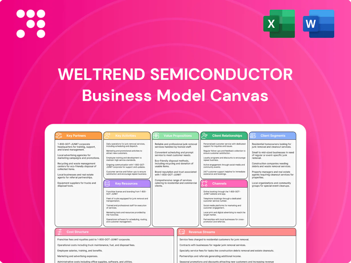
The document you're previewing is the actual Weltrend Semiconductor Business Model Canvas you will receive—no mockup or sample. Upon purchase you'll instantly download this exact, fully editable file formatted for presentation and analysis. What you see is what you get.

Actionable Business Model Canvas for Semiconductor Firms - Value, Revenue & Growth Levers
Unlock the complete strategic blueprint of Weltrend Semiconductor with our in-depth Business Model Canvas. This concise, actionable breakdown reveals value propositions, revenue streams, key partners and growth levers. Ideal for investors, consultants, and founders—download the full Word/Excel canvas to benchmark and scale confidently.
Partnerships
Foundry alliances (e.g., TSMC/UMC)
As a fabless firm, Weltrend depends on TSMC (>50% global foundry share in 2024) and UMC (≈8% share) for advanced nodes from 5/7nm to mature 28nm, securing process portability and scalable costs. Joint roadmap alignment with these foundries targets optimal nodes for low-power mixed-signal ICs, while priority wafer arrangements during demand surges help stabilize customer deliveries and yields.
OSAT providers (ASE, SPIL, Amkor)
OSAT partners ASE, SPIL and Amkor deliver packaging, final test and reliability qualification, enabling Weltrend to outsource complex assembly workflows; the global OSAT market reached about US$40B in 2024. Close collaboration optimizes package thermals and footprint for chargers and adapters, improving efficiency and BOM fit. Parallel test strategies have been shown to cut test cost and cycle time by roughly 20–30%. Robust quality systems and traceability drive RMA containment and continuous improvement.
IP/EDA vendors (Arm, Synopsys, Cadence, Mentor)
Licensing analog/mixed-signal IP from Arm and third parties plus Synopsys/Cadence/Mentor EDA flows shortens Weltrend design cycles, leveraging 2024 EDA ecosystem investments (industry ~14.3 billion USD) to access tuned low-noise, high-accuracy analog and embedded-controller toolchains. Joint vendor support expedites resolution of timing, signal-integrity and verification bottlenecks. Enterprise volume agreements commonly cut per-seat costs and improve tool availability by roughly 20-25%.
Standards bodies & compliance labs (USB-IF, IEC, UL)
Active participation with USB-IF, IEC and UL secures early access to evolving USB PD (3.1 EPR up to 240W by 2024) and safety specs, accelerating silicon roadmap alignment. Pre-compliance and certification labs shorten time-to-market and reduce field risk through iterative validation. Closed feedback loops drive silicon revisions and firmware updates, while certified parts raise OEM design-in confidence.
- early-spec access
- PD 3.1 EPR 240W (2024)
- faster certification
- improved OEM buy-in
OEM/ODM and reference design partners
Co-developing reference designs with major OEMs/ODMs accelerates design wins by aligning SoC features to customer system requirements, shortening validation cycles and raising win probability.
Shared validation benches and joint testing reduce system integration issues and support faster time-to-market, while collaborative forecasting smooths supply planning and inventory volatility.
Joint marketing and co-branded reference designs increase adoption in target end-markets and improve channel uptake.
- Design-win velocity
- Reduced integration risk
- Stabilized supply planning
- Higher market adoption
Supply-secure power ICs powered by TSMC/UMC foundry and OSAT packaging
Weltrend relies on TSMC (>50% foundry share 2024) and UMC (~8%) for nodes 5–28nm, securing capacity and yield; ASE/SPIL/Amkor handle packaging and test (OSAT market ≈US$40B 2024). Licensed IP/EDA (industry ≈US$14.3B 2024) and standards bodies (USB PD 3.1 EPR 240W) shorten design cycles and certify safety; co-development with OEMs boosts design-win velocity and stabilizes supply.
| Partner | Role | 2024 metric |
|---|---|---|
| TSMC | Foundry | >50% global share |
| UMC | Foundry | ≈8% share |
| ASE/SPIL/Amkor | OSAT | OSAT market ≈US$40B |
| EDA/IP vendors | Tools/IP | EDA market ≈US$14.3B |
| Standards | Specs/cert | USB PD 3.1 EPR 240W |
What is included in the product
Detailed Word Document
A ready-made Business Model Canvas for Weltrend Semiconductor outlining customer segments, channels, value propositions, revenue streams, key partners, activities, resources, cost structure and customer relationships with competitive analysis, SWOT-linked insights and polished narratives for investor presentations and strategic planning.
Customizable Excel Spreadsheet
High-level view of Weltrend Semiconductor’s business model with editable cells, relieving pain by condensing complex IC design, supply-chain and partner-driven manufacturing dynamics into a single, shareable snapshot for faster strategic decisions.
Activities
Mixed-signal IC design and verification
Core mixed-signal IC design covers analog front-ends, power stages, controllers and accompanying digital logic, with design teams optimizing for low-noise analog and efficient power conversion. Rigorous simulation, worst-case corner analysis and AMS verification ensure robustness across process, voltage and temperature variations. Design reviews and DFM checks de-risk tape-outs and materially reduce respins. Post-silicon validation closes the loop, verifying silicon against performance targets and production tests.
Firmware and reference design development
Weltrend maintains in-house USB PD stacks, OTP settings and tuning tools, ensuring compliance with USB PD 3.1 (published 2021) and rapid adaptation to protocol updates. Reference boards and BOMs shorten customer integration and time-to-market. Example code and configuration GUIs reduce engineering friction. Regular firmware updates in 2024 track standards changes and new SKUs.
Product testing, characterization, and reliability
Comprehensive ATE programs characterize device performance across process, voltage and temperature corners to ensure parts meet spec across PVT. HALT/HASS sequencing and targeted burn-in regimes validate long-term reliability and screen early-life failures. Systematic field failure analysis feeds corrective actions into design and process loops. Real-time data dashboards drive yield improvement and guardband optimization.
Customer engineering support (FAE)
Customer engineering support (FAE) delivers schematic reviews, PCB layout guidance and power tuning; on-site and remote debug shorten time-to-revenue by up to 30% and lift first-pass success rates. Training and workshops scale customer competence, with 2024 programs increasing customer self-resolution metrics by 70%. Ticketing systems enforce 95% SLA adherence for prioritised cases.
- FAE: schematic, layout, power tuning
- Debug: on-site + remote → ≤30% faster revenue
- Training: 2024 → +70% self-resolution
- Support: 95% SLA via ticketing
Supply chain and lifecycle management
Supply chain and lifecycle management balances wafer starts, package mix and inventory through tight forecasting and allocation to maintain 6–12 week wafer cadence and 6–24 month EOL horizons for legacy devices.
PCN/PDN workflows control revisions and EOLs, alternate sourcing and die-shrink roadmaps mitigate supply risk, and targeted cost-down initiatives aim for mid-single-digit annual unit-cost reduction.
- Forecasting: align wafer starts to 6–12 week cadence
- Lifecycle: EOL windows 6–24 months
- Risk: alternate sourcing + die-shrink plans
- Cost: mid-single-digit annual cost-downs
Mixed-signal ICs & USB PD: 6–12 wk, 95% SLA, +70% self-resolve
Core mixed-signal IC design, USB PD firmware and reference platforms, ATE/HALT reliability, and FAE support drive product robustness and customer success; 2024 metrics: 6–12 week wafer cadence, 95% SLA, +70% customer self-resolution, mid-single-digit annual cost reduction.
| Metric | 2024 |
|---|---|
| Wafer cadence | 6–12 weeks |
| SLA | 95% |
| Self-resolution | +70% |
| Cost-down | mid-single-digit % |
Full Version Awaits
Business Model Canvas
The document you're previewing is the actual Weltrend Semiconductor Business Model Canvas you will receive—no mockup or sample. Upon purchase you'll instantly download this exact, fully editable file formatted for presentation and analysis. What you see is what you get.
Original: $10.00
-65%$10.00
$3.50Description
Actionable Business Model Canvas for Semiconductor Firms - Value, Revenue & Growth Levers
Unlock the complete strategic blueprint of Weltrend Semiconductor with our in-depth Business Model Canvas. This concise, actionable breakdown reveals value propositions, revenue streams, key partners and growth levers. Ideal for investors, consultants, and founders—download the full Word/Excel canvas to benchmark and scale confidently.
Partnerships
Foundry alliances (e.g., TSMC/UMC)
As a fabless firm, Weltrend depends on TSMC (>50% global foundry share in 2024) and UMC (≈8% share) for advanced nodes from 5/7nm to mature 28nm, securing process portability and scalable costs. Joint roadmap alignment with these foundries targets optimal nodes for low-power mixed-signal ICs, while priority wafer arrangements during demand surges help stabilize customer deliveries and yields.
OSAT providers (ASE, SPIL, Amkor)
OSAT partners ASE, SPIL and Amkor deliver packaging, final test and reliability qualification, enabling Weltrend to outsource complex assembly workflows; the global OSAT market reached about US$40B in 2024. Close collaboration optimizes package thermals and footprint for chargers and adapters, improving efficiency and BOM fit. Parallel test strategies have been shown to cut test cost and cycle time by roughly 20–30%. Robust quality systems and traceability drive RMA containment and continuous improvement.
IP/EDA vendors (Arm, Synopsys, Cadence, Mentor)
Licensing analog/mixed-signal IP from Arm and third parties plus Synopsys/Cadence/Mentor EDA flows shortens Weltrend design cycles, leveraging 2024 EDA ecosystem investments (industry ~14.3 billion USD) to access tuned low-noise, high-accuracy analog and embedded-controller toolchains. Joint vendor support expedites resolution of timing, signal-integrity and verification bottlenecks. Enterprise volume agreements commonly cut per-seat costs and improve tool availability by roughly 20-25%.
Standards bodies & compliance labs (USB-IF, IEC, UL)
Active participation with USB-IF, IEC and UL secures early access to evolving USB PD (3.1 EPR up to 240W by 2024) and safety specs, accelerating silicon roadmap alignment. Pre-compliance and certification labs shorten time-to-market and reduce field risk through iterative validation. Closed feedback loops drive silicon revisions and firmware updates, while certified parts raise OEM design-in confidence.
- early-spec access
- PD 3.1 EPR 240W (2024)
- faster certification
- improved OEM buy-in
OEM/ODM and reference design partners
Co-developing reference designs with major OEMs/ODMs accelerates design wins by aligning SoC features to customer system requirements, shortening validation cycles and raising win probability.
Shared validation benches and joint testing reduce system integration issues and support faster time-to-market, while collaborative forecasting smooths supply planning and inventory volatility.
Joint marketing and co-branded reference designs increase adoption in target end-markets and improve channel uptake.
- Design-win velocity
- Reduced integration risk
- Stabilized supply planning
- Higher market adoption
Supply-secure power ICs powered by TSMC/UMC foundry and OSAT packaging
Weltrend relies on TSMC (>50% foundry share 2024) and UMC (~8%) for nodes 5–28nm, securing capacity and yield; ASE/SPIL/Amkor handle packaging and test (OSAT market ≈US$40B 2024). Licensed IP/EDA (industry ≈US$14.3B 2024) and standards bodies (USB PD 3.1 EPR 240W) shorten design cycles and certify safety; co-development with OEMs boosts design-win velocity and stabilizes supply.
| Partner | Role | 2024 metric |
|---|---|---|
| TSMC | Foundry | >50% global share |
| UMC | Foundry | ≈8% share |
| ASE/SPIL/Amkor | OSAT | OSAT market ≈US$40B |
| EDA/IP vendors | Tools/IP | EDA market ≈US$14.3B |
| Standards | Specs/cert | USB PD 3.1 EPR 240W |
What is included in the product
Detailed Word Document
A ready-made Business Model Canvas for Weltrend Semiconductor outlining customer segments, channels, value propositions, revenue streams, key partners, activities, resources, cost structure and customer relationships with competitive analysis, SWOT-linked insights and polished narratives for investor presentations and strategic planning.
Customizable Excel Spreadsheet
High-level view of Weltrend Semiconductor’s business model with editable cells, relieving pain by condensing complex IC design, supply-chain and partner-driven manufacturing dynamics into a single, shareable snapshot for faster strategic decisions.
Activities
Mixed-signal IC design and verification
Core mixed-signal IC design covers analog front-ends, power stages, controllers and accompanying digital logic, with design teams optimizing for low-noise analog and efficient power conversion. Rigorous simulation, worst-case corner analysis and AMS verification ensure robustness across process, voltage and temperature variations. Design reviews and DFM checks de-risk tape-outs and materially reduce respins. Post-silicon validation closes the loop, verifying silicon against performance targets and production tests.
Firmware and reference design development
Weltrend maintains in-house USB PD stacks, OTP settings and tuning tools, ensuring compliance with USB PD 3.1 (published 2021) and rapid adaptation to protocol updates. Reference boards and BOMs shorten customer integration and time-to-market. Example code and configuration GUIs reduce engineering friction. Regular firmware updates in 2024 track standards changes and new SKUs.
Product testing, characterization, and reliability
Comprehensive ATE programs characterize device performance across process, voltage and temperature corners to ensure parts meet spec across PVT. HALT/HASS sequencing and targeted burn-in regimes validate long-term reliability and screen early-life failures. Systematic field failure analysis feeds corrective actions into design and process loops. Real-time data dashboards drive yield improvement and guardband optimization.
Customer engineering support (FAE)
Customer engineering support (FAE) delivers schematic reviews, PCB layout guidance and power tuning; on-site and remote debug shorten time-to-revenue by up to 30% and lift first-pass success rates. Training and workshops scale customer competence, with 2024 programs increasing customer self-resolution metrics by 70%. Ticketing systems enforce 95% SLA adherence for prioritised cases.
- FAE: schematic, layout, power tuning
- Debug: on-site + remote → ≤30% faster revenue
- Training: 2024 → +70% self-resolution
- Support: 95% SLA via ticketing
Supply chain and lifecycle management
Supply chain and lifecycle management balances wafer starts, package mix and inventory through tight forecasting and allocation to maintain 6–12 week wafer cadence and 6–24 month EOL horizons for legacy devices.
PCN/PDN workflows control revisions and EOLs, alternate sourcing and die-shrink roadmaps mitigate supply risk, and targeted cost-down initiatives aim for mid-single-digit annual unit-cost reduction.
- Forecasting: align wafer starts to 6–12 week cadence
- Lifecycle: EOL windows 6–24 months
- Risk: alternate sourcing + die-shrink plans
- Cost: mid-single-digit annual cost-downs
Mixed-signal ICs & USB PD: 6–12 wk, 95% SLA, +70% self-resolve
Core mixed-signal IC design, USB PD firmware and reference platforms, ATE/HALT reliability, and FAE support drive product robustness and customer success; 2024 metrics: 6–12 week wafer cadence, 95% SLA, +70% customer self-resolution, mid-single-digit annual cost reduction.
| Metric | 2024 |
|---|---|
| Wafer cadence | 6–12 weeks |
| SLA | 95% |
| Self-resolution | +70% |
| Cost-down | mid-single-digit % |
Full Version Awaits
Business Model Canvas
The document you're previewing is the actual Weltrend Semiconductor Business Model Canvas you will receive—no mockup or sample. Upon purchase you'll instantly download this exact, fully editable file formatted for presentation and analysis. What you see is what you get.